TFT-LCD (thin film transistor-liquid crystal display) array substrate and manufacturing method thereof
A technology of an array substrate and a manufacturing method, applied in the field of liquid crystal display, can solve the problems of source electrode and active layer transmission obstruction, and achieve the effects of reducing the number of processes, improving market competitiveness, and saving costs
- Summary
- Abstract
- Description
- Claims
- Application Information
AI Technical Summary
Problems solved by technology
Method used
Image

Examples
Embodiment 1
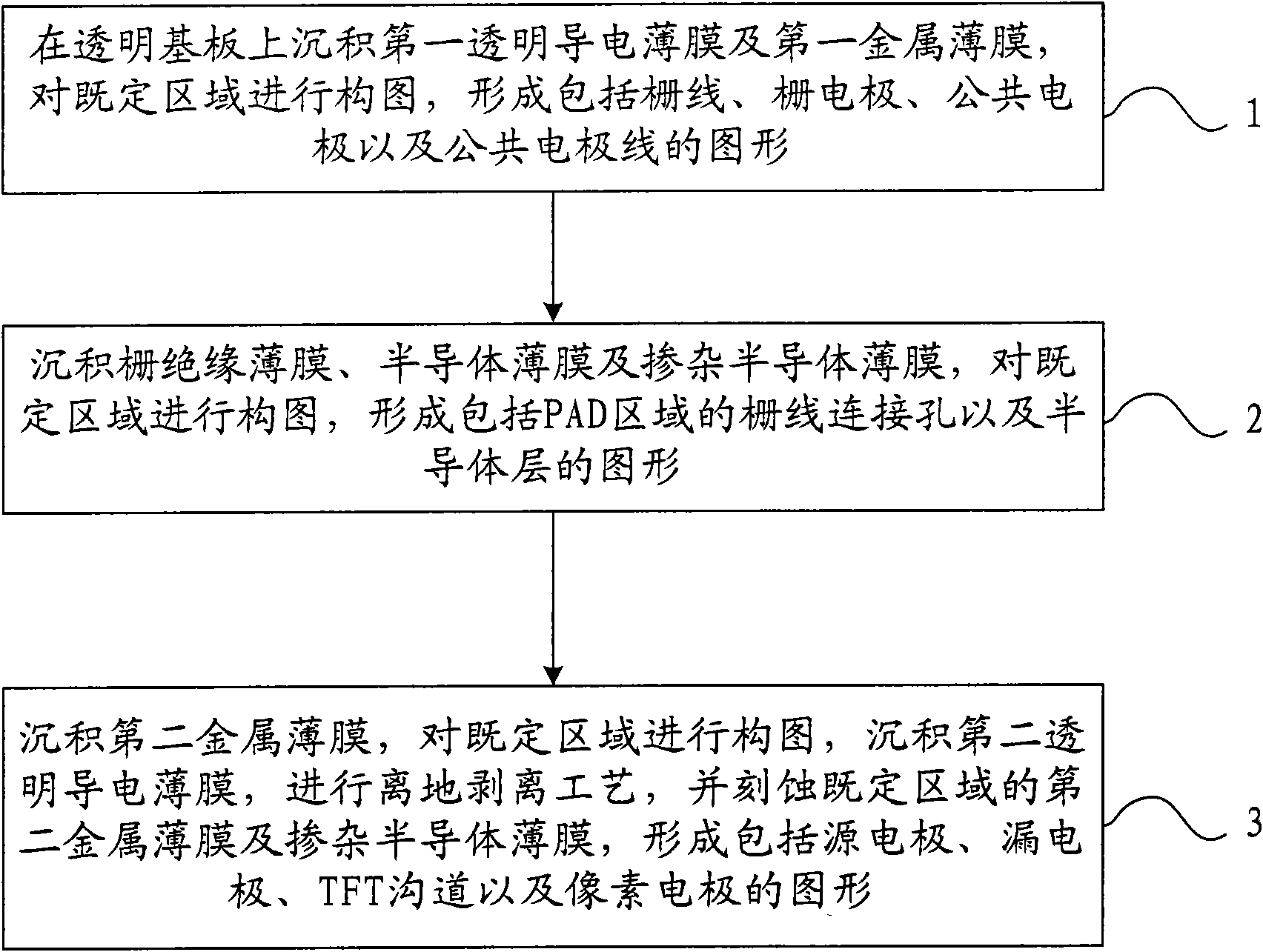
[0086] figure 2 It is a flow chart of Embodiment 1 of the manufacturing method of the TFT-LCD array substrate of the present invention. Such as figure 2 Shown, the manufacturing method of TFT-LCD array substrate of the present invention comprises:
[0087] Step 1, depositing a first transparent conductive film and a first metal film on a transparent substrate, patterning a predetermined area, and forming a pattern including gate lines, gate electrodes, common electrodes and common electrode lines;
[0088] Step 2, depositing a gate insulating film, a semiconductor film and a doped semiconductor film, patterning a predetermined area, and forming a gate connection hole including a PAD area and a pattern of a semiconductor layer;
[0089] Step 3. Deposit the second metal film, pattern the predetermined area, deposit the second transparent conductive film, perform the lift-off process, and etch the second metal film and the doped semiconductor film in the predetermined area to...
Embodiment 2
[0118] Figure 22 It is a flow chart of Embodiment 2 of the manufacturing method of the TFT-LCD array substrate of the present invention. Such as Figure 22 Shown, the manufacturing method of TFT-LCD array substrate of the present invention comprises:
[0119] Step 100, depositing a first transparent conductive film and a first metal film on a transparent substrate, patterning a predetermined area to form a pattern including gate lines, gate electrodes, pixel electrodes and common electrode lines;
[0120] Step 200, depositing a gate insulating film, a semiconductor film, and a doped semiconductor film, patterning a predetermined area, and forming a pattern including via holes, gate connection holes in the PAD area, and a semiconductor layer;
[0121] Step 300, depositing a second metal film, patterning a predetermined area, depositing a second transparent conductive film, performing a lift-off process, and etching the second metal film and a doped semiconductor film in a pr...
PUM
 Abstract
Description
Claims
Application Information
 - R&D
- Intellectual Property
- Life Sciences
- Materials
- Tech Scout
- Unparalleled Data Quality
- Higher Quality Content
- 60% Fewer Hallucinations
Browse by: Latest US Patents, China's latest patents, Technical Efficacy Thesaurus, Application Domain, Technology Topic, Popular Technical Reports.
© 2025 PatSnap. All rights reserved.Legal|Privacy policy|Modern Slavery Act Transparency Statement|Sitemap|About US| Contact US: help@patsnap.com