Semiconductor packing structure applied to power switcher circuit

A packaging structure, semiconductor technology, applied in the direction of semiconductor devices, semiconductor/solid-state device components, circuits, etc., can solve the problem of bypass capacitor CMOSFET, save packaging space, improve the performance of DC-DC converters, and reduce the number of Effect

Active Publication Date: 2011-08-31
ALPHA & OMEGA SEMICON INT LP
View PDF8 Cites 7 Cited by
  • Summary
  • Abstract
  • Description
  • Claims
  • Application Information

AI Technical Summary

Problems solved by technology

[0004] However, in the current semiconductor packaging technology, two MOSFETs are packaged in the same semiconductor package to form a power switch, and then the bypass circuit C and the PIC chip are connected in parallel outside the package, thus causing the bypass capacitor C The setting position of the MOSFET is relatively far away from the MOSFET, so it cannot play its role better

Method used


Image

  • Semiconductor packing structure applied to power switcher circuit
  • Semiconductor packing structure applied to power switcher circuit
  • Semiconductor packing structure applied to power switcher circuit

Examples


Embodiment 1

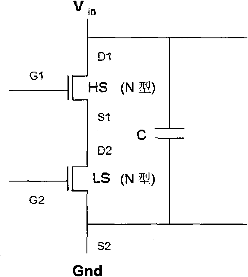
[0049] In this embodiment, the high-end MOSFET chip is stacked on the low-end MOSFET chip, and the bypass capacitor is connected in parallel, and the connecting leads are used to make corresponding electrical connections. Finally, the three circuit elements are mixed and packaged in the same semiconductor package. Realization basis figure 1 The circuit diagram is connected to form the power switch.

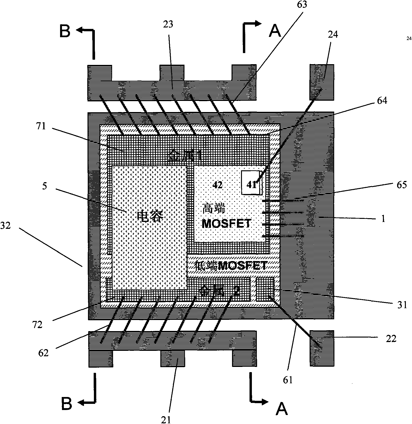
[0050] Such as Figure 3A Shown is a top view of Embodiment 1 provided by the present invention; Figure 3B For along Figure 3A A cross-sectional view in the A-A direction. The package includes a lead frame with a carrier 1 and a number of pins. According to figure 1 In the circuit diagram of the power switch shown, the pins include a low-end source pin 21, a low-end gate pin 22, a high-end drain pin 23, and a high-end gate pin 24, where these leads The feet are separated from the slide table 1 and electrically connected. The low-side MOSFET 3 is glued and attached to the stage 1,...

Embodiment 2

[0054] Figure 4A It is a top view of Embodiment 2 provided by the present invention; Figure 4B For along Figure 4A Sectional view in the A-A direction; Figure 4C For along Figure 4A Sectional view in the direction of B-B. This embodiment 2 is basically the same as the package structure described in the above embodiment 1, except that: in this embodiment, a metal connection plate 62' (or a metal connection body such as a metal connection tape) is used instead of implementation. Several connecting leads 62 in Example 1 are used to bond and connect the first metal layer 71 and the low-end source pin 21, and a metal connecting plate 63' is used instead of several connecting leads 63 in Example 1 to bond and connect the second metal layer. For 72 and the high-side drain pin 23, a metal connecting plate 65' is used instead of the several connecting leads 65 in the first embodiment to bond and connect the top source 42 of the high-side MOSFET 4 and the stage 1.

[0055] Similarly, ...

Embodiment 3

[0058] The package structure features provided by the third embodiment are still similar to those of the first embodiment. The core structure is still to stack the high-end MOSFET chip on the low-end MOSFET chip, but in this embodiment, a vertical structure capacitor element is used. The electrodes at both ends of the capacitive element are respectively located on the top surface and the bottom surface.

[0059] Figure 5A It is a top view of Embodiment 3 provided by the present invention; Figure 5B For along Figure 5A A cross-sectional view in the A-A direction. Wherein, the lead frame structure is as shown in embodiment 1, including a stage 1 and a number of pins that are separated from the stage 1 and are not electrically connected; these pins include low-end source pins 21, Low-side gate pin 22, high-side drain pin 23, and high-side gate pin 24. The low-end MOSFET 3 is glued and attached to the stage 1, and its bottom drain (not shown in the figure) is electrically connect...


PUM


Abstract

The invention discloses a semiconductor packaging structure applied to a power switcher circuit. A power switcher is formed by stacking and connecting two MOSFET (Metal-Oxide -Semiconductor Field Effect Transistor) chips, and a bypass capacitor is packaged in the same package horizontally or vertically; moreover, a PIC (Positive-Impedance Converter) chip is arranged in the same package for forming a DC-DC (Direct Current to Direct Current) switcher. The semiconductor packaging structure provided by the invention ensures that the bypass capacitor is closest to the MOSFET chip, the generated parasitic inductance is the minimum, and thus the size of the semiconductor structure is effectively reduced while the performance of the power switcher or DC-DC switcher is effectively improved.

Description

Technical field [0001] The present invention relates to a semiconductor package, in particular to a semiconductor package structure applied to a power switch circuit in which multiple chips and circuit elements such as capacitors are all packaged in the same semiconductor package. Background technique [0002] Such as figure 1 Shown is the circuit diagram of a power switch formed by connecting two N-type MOSFETs, where the drain D1 of the high-side MOSFET (HS) is connected to the Vin terminal, and the source S1 is connected to the drain D2 of the low-side MOSFET (LS), and The source S2 of the low-side MOSFET is connected to the Gnd end. Usually, a bypass circuit C is also provided in parallel between the Vin-Gnd ends of the power switch, and the capacitor is set to suppress the voltage impulse when the power switch is started, so as to improve the performance of the power switch . Further, such as figure 2 As shown, a power controller (PIC) is connected in parallel at both end...

Claims


Application Information

Patent Timeline
Patent Type & Authority Applications(China)
IPC IPC(8): H01L25/00H01L23/495H01L23/482H01L23/488H02M3/10
CPCH01L24/34H01L2224/48091H01L2224/48247H01L2224/48137H01L2924/13091H01L2924/3011H01L2924/30107H01L2924/1306H01L2224/40095H01L2224/40245H01L2224/32245H01L2224/48257H01L2224/49111H01L2224/73221H01L2224/73265H01L2224/371H01L2224/83801H01L2224/37H01L2924/00014H01L2224/40H01L24/37H01L2924/00H01L2224/84
Inventor 薛彦迅安荷·叭剌鲁军
Owner ALPHA & OMEGA SEMICON INT LP
Why Eureka
Try Eureka