Layout structure for shift buffer circuit

A shift register, layout structure technology, applied in circuits, static memory, digital memory information and other directions, can solve the problems of increasing circuit layout density, insufficient layout space, etc., to improve circuit layout density, alleviate insufficient circuit layout space, The effect of improving power consumption

Inactive Publication Date: 2011-09-14
AU OPTRONICS CORP
View PDF2 Cites 2 Cited by
  • Summary
  • Abstract
  • Description
  • Claims
  • Application Information

AI Technical Summary

Problems solved by technology

[0005] One of the purposes of the present invention is to provide a layout structure of a shift register circuit to solve the problem of insufficient layout space in circuit design in the prior art or to increase the layout density of the circuit

Method used


Image

  • Layout structure for shift buffer circuit
  • Layout structure for shift buffer circuit
  • Layout structure for shift buffer circuit

Examples


Embodiment Construction

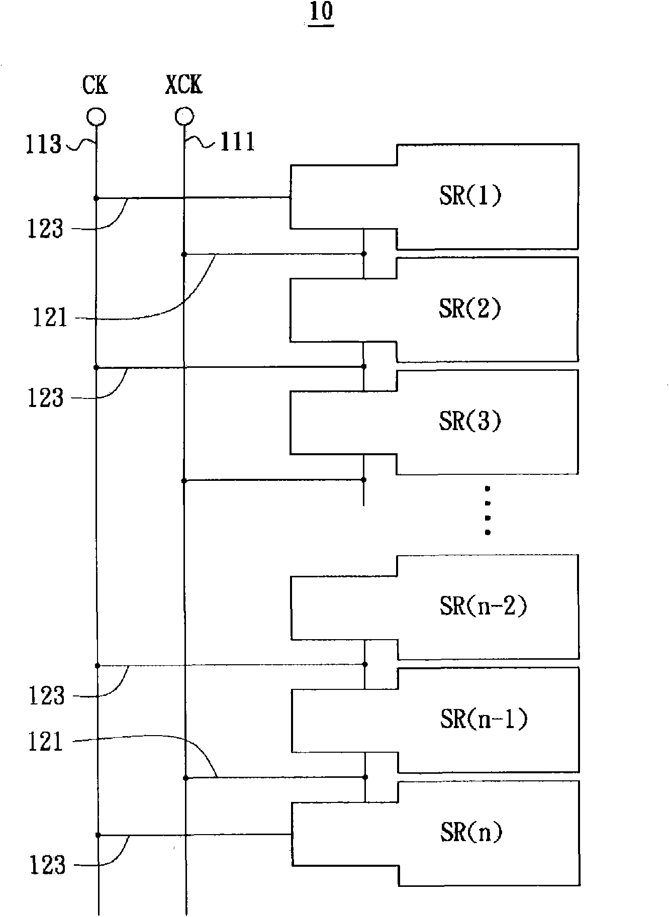
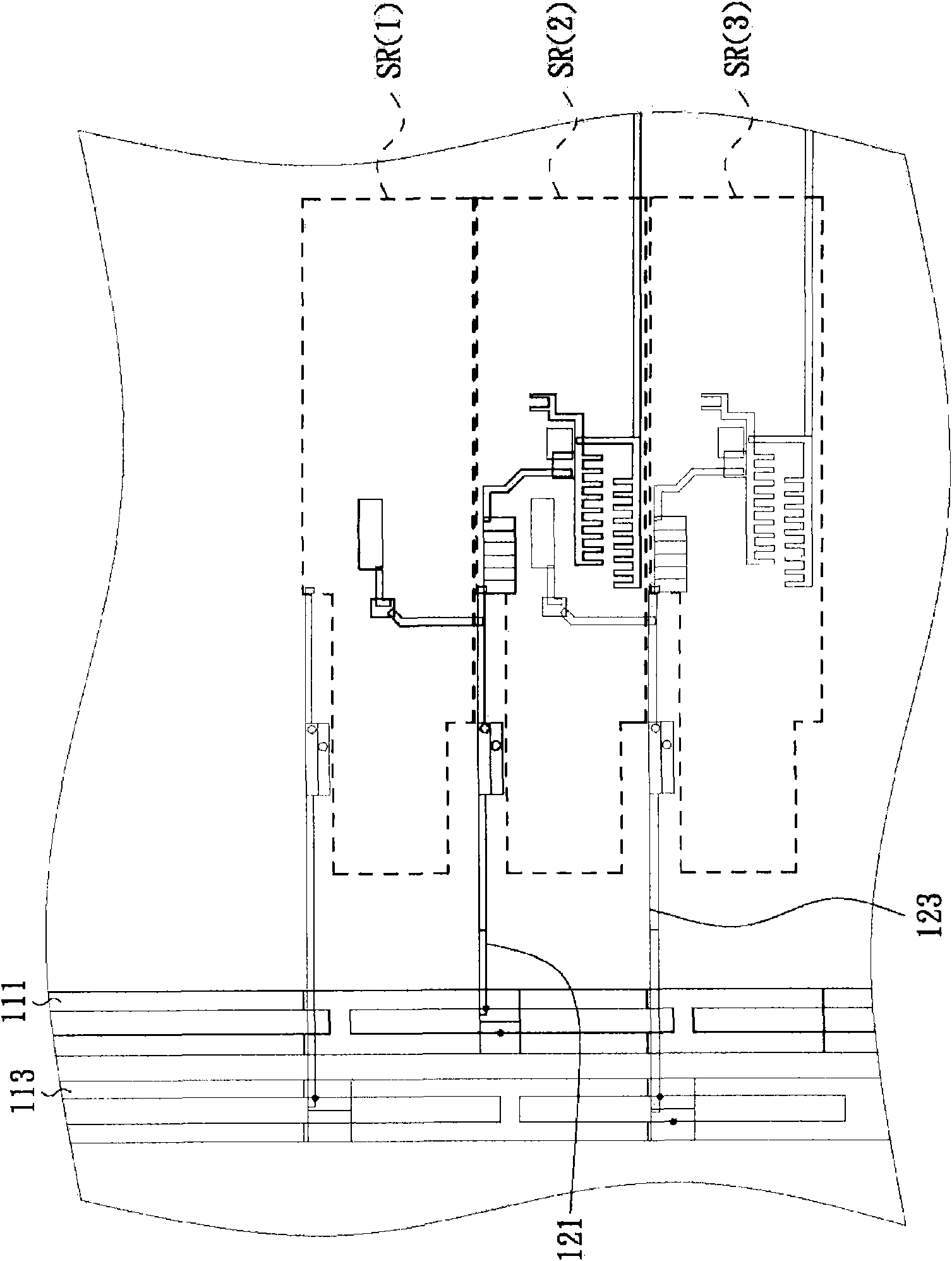
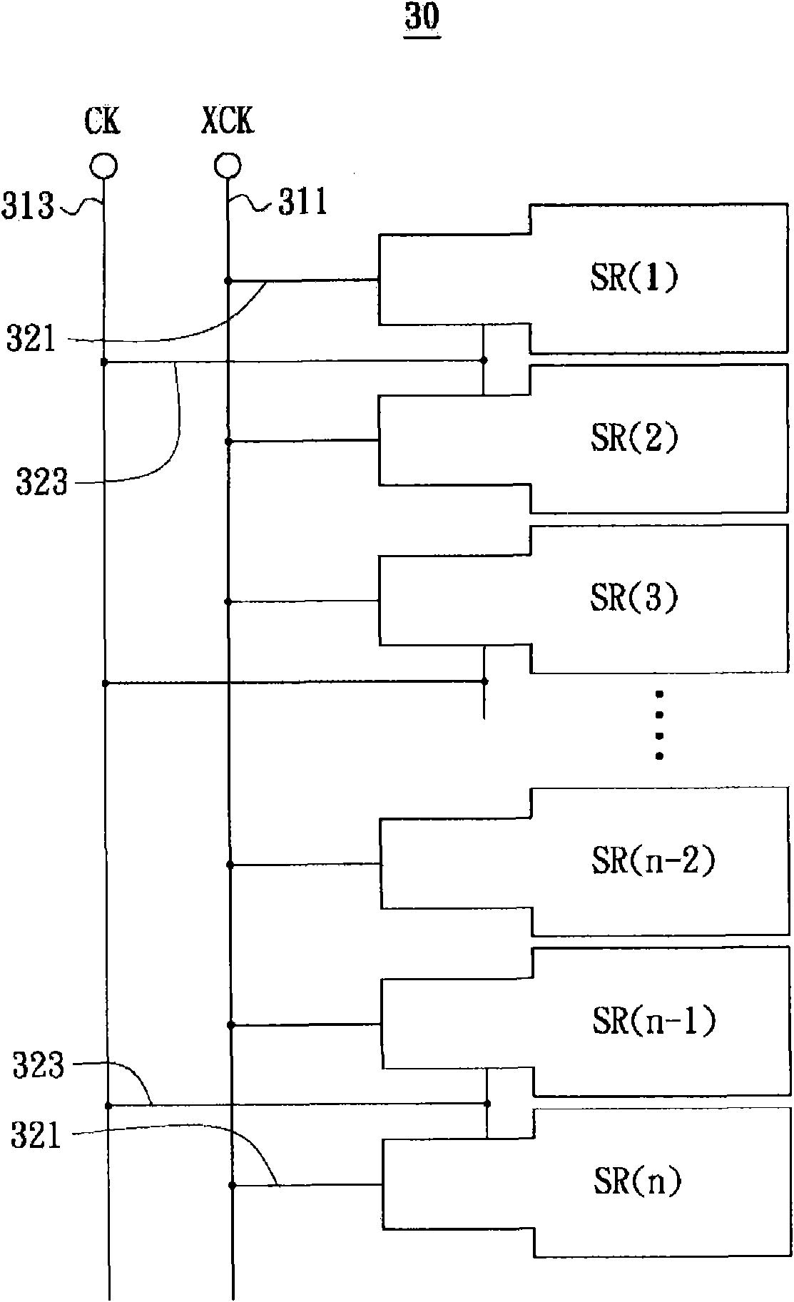
[0026] see figure 1 , which shows a schematic diagram of the principle of a layout structure of a shift register circuit proposed in an embodiment of the present invention. Such as figure 1 As shown, the shift register circuit 10 includes: shift registers SR(1), SR(2), SR(3)...SR(n-2), SR(n-1), SR(n), signal The traces 121 , 123 and the bus lines 111 , 113 arranged parallel to each other; wherein n is a positive integer greater than 1. Here, the shift register circuit 10 can be applied to an array gate-type gate drive circuit of a display, but the present invention is not limited thereto, and it can also be applied to other drive circuits such as chip-type gate drive circuits or Chip-type source driver circuits, etc.

[0027] Based on the above, each shift register SR(1), SR(2), SR(3)...SR(n-2), SR(n-1), SR(n) in this embodiment all receive clock Signals XCK and CK, and every two adjacent shift registers SR(1), SR(2), SR(3)...SR(n-2), SR(n-1), SR(n) share one signal routi...


PUM


Abstract

The invention relates to a layout structure for shift buffer circuits, which comprises a first shift buffer and a second shift buffer arranged adjacent to the first shift buffer. A first signal and a second signal are received by the first shift buffer and the second shift buffer. The second signal and the first signal are reversed phases to each other. In addition, the first shift buffer and the second shift buffer share the signal line so as to receive the first signal. The shared signal line extends between the first shift buffer and the second shift buffer.

Description

【Technical field】 [0001] The invention relates to the technical field of semiconductor manufacturing process, and in particular to a layout structure of a shift register circuit. 【Background technique】 [0002] Press, flat-panel displays such as liquid crystal displays are widely used in consumer electronics products such as mobile phones, notebook computers, desktop displays, and televisions due to their advantages of high image quality, small size, light weight, and wide application range, and have been Gradually replace the traditional cathode ray tube (CRT) display and become the mainstream of the display. [0003] In the liquid crystal display panel, a gate drive circuit and a source drive circuit are provided to respectively provide a gate drive pulse signal and a display data signal, thereby achieving the purpose of image display. In the gate driving circuit and the source driving circuit, a shift register circuit is usually provided for shifting and temporarily stor...

Claims


Application Information

Patent Timeline
Patent Type & Authority Applications(China)
IPC IPC(8): G09G3/20G09G3/36
CPCG11C19/28G09G3/3674G09G2310/0286H01L24/01
Inventor 陈盈真李豪捷张竣桓刘俊欣陈婉蓉
Owner AU OPTRONICS CORP
Why Eureka
Try Eureka