Power mos tube and its manufacturing method

A technology of a MOS tube and a manufacturing method, which is applied in the field of power MOS tube and its manufacturing, can solve the problems of avalanche breakdown and small breakdown voltage of the power MOS tube, so as to improve the breakdown voltage, reduce the parasitic capacitance, and reduce the power line density. Effect

Active Publication Date: 2016-03-02
SHANGHAI HUAHONG GRACE SEMICON MFG CORP
View PDF14 Cites 0 Cited by
  • Summary
  • Abstract
  • Description
  • Claims
  • Application Information

AI Technical Summary

Problems solved by technology

[0015] As mentioned above, in the prior art power MOS tube, the surface closest to the U-shaped gate 105 and the drain region 101 is the bottom end surface of the entire U-shaped gate 105, because the U-shaped gate 105 The gate oxide layer on the bottom surface of the U-shaped trench is thinner. When a high voltage is applied to the substrate, the electric force lines at the bottom of the U-shaped trench are the densest, so the electric field is the strongest at the bottom of the U-shaped trench, making it easy for the power MOS transistor to be placed in the U-shaped trench. Avalanche breakdown occurs at the bottom of the slot, resulting in a small breakdown voltage

Method used


Image

  • Power mos tube and its manufacturing method
  • Power mos tube and its manufacturing method
  • Power mos tube and its manufacturing method

Examples


Embodiment Construction

[0036] The following will combine image 3 ~ FIG. 5 further describes in detail the power MOS transistor and its manufacturing method of the present invention.

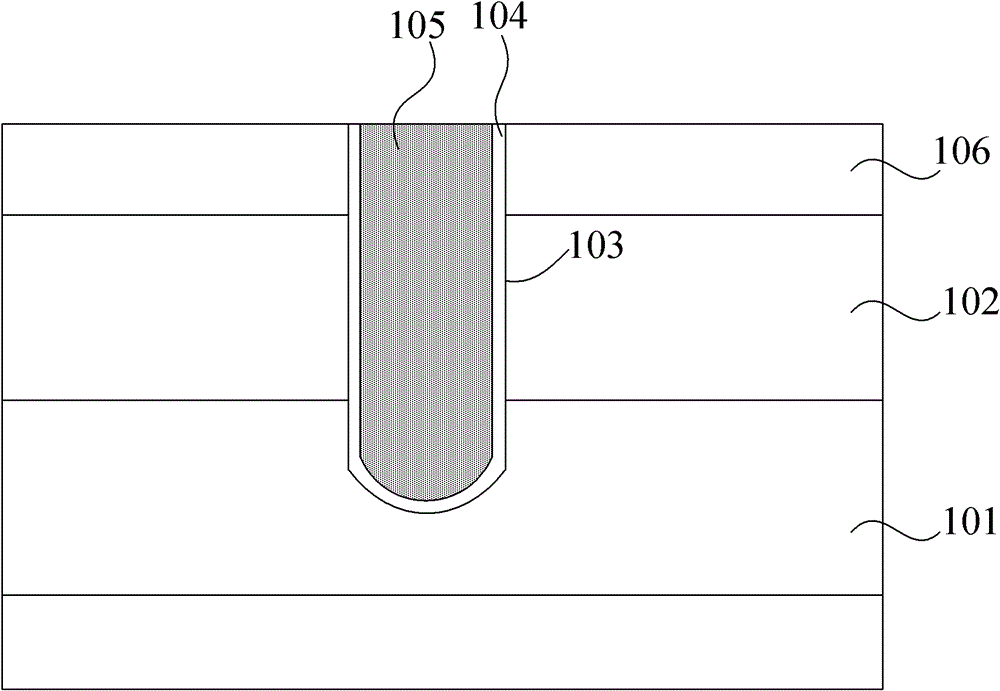
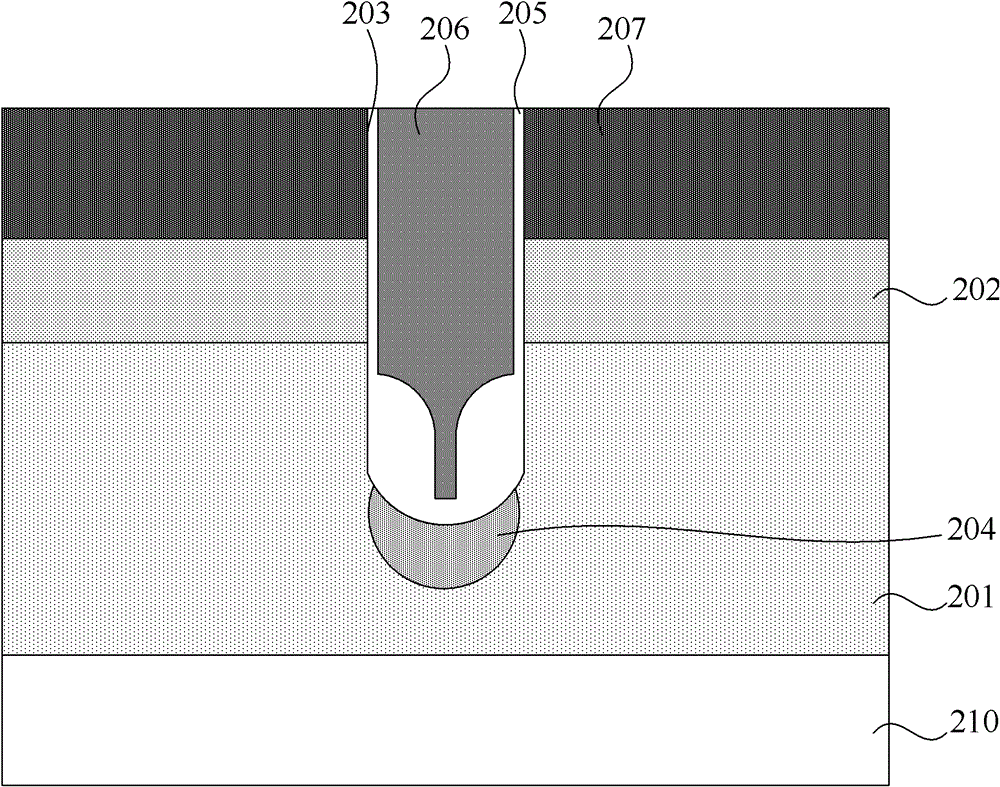
[0037] see image 3 The power MOS transistor of the present invention includes a drain region 201, a body region 202 formed on the drain region 201, a U-shaped gate trench 203 arranged in the body region 202 and the drain region 201, and arranged in the The side wall of the U-shaped gate trench 203 and the gate oxide layer 205 at the bottom end fill the gate 206 formed by the U-shaped gate trench 203, and are arranged in the drain region 201, close to the U-shaped gate. The floating ring 204 at the bottom of the pole trench 203, and the source region 207 arranged on both sides of the U-shaped gate trench 203 and below the surface of the body region 202, wherein the bottom of the U-shaped gate trench 203 The surface of the gate oxide layer 205 is approximately V-shaped, and the bottom end surface of the gate 206 is a...


PUM


Abstract

The present invention relates to a power MOS transistor and a manufacturing method thereof. The power MOS transistor includes a drain region, a body region formed on the drain region, and a U-shaped gate trench arranged in the body region and the drain region. The gate oxide layer on the sidewall and bottom of the U-shaped gate trench fills the gate formed by the U-shaped gate trench, and is arranged on both sides of the U-shaped gate trench, the body In the source region below the surface of the region, a floating ring is provided in the drain region, adjacent to the bottom of the U-shaped gate trench, and the surface of the gate oxide layer at the bottom of the U-shaped gate trench is approximately V-shaped, The bottom end face of the gate is a V-shaped end face. The power MOS tube and the manufacturing method thereof of the present invention make the electric field on the side wall of the U-shaped trench evenly distributed by setting the V-shaped oxide layer at the bottom of the U-shaped gate trench and the floating ring in the drain region, thereby improving the power MOS tube. breakdown voltage.

Description

technical field [0001] The invention relates to a semiconductor manufacturing process, in particular to a power MOS tube and a manufacturing method thereof. Background technique [0002] figure 1 Shown is a cross-sectional view of a power MOS transistor in the prior art. The power MOS transistor includes: a drain region 101, a body region 102 formed on the drain region 101, and a U-shaped gate trench 103, a U-shaped gate oxide layer 104 disposed on the sidewall and bottom of the U-shaped gate trench 103, filling the U-shaped gate 105 formed by the U-shaped gate trench 103, and a source region 106 disposed on both sides of the U-shaped gate trench 103 and below the surface of the body region 102 . [0003] figure 2 Shown is the manufacturing flowchart of the above-mentioned power MOS tube, and the manufacturing method of the power MOS tube in the prior art includes the following steps: [0004] Step S101, providing a heavily doped semiconductor substrate, forming an epit...

Claims


Application Information

Patent Timeline
Patent Type & Authority Patents(China)
IPC IPC(8): H01L29/78H01L29/423H01L21/336
CPCH01L29/7813H01L29/0623H01L29/42376H01L29/66734
Inventor 苟鸿雁吴小利
Owner SHANGHAI HUAHONG GRACE SEMICON MFG CORP
Why Eureka
Try Eureka