Wafer level package method

A wafer-level packaging and packaging layer technology, applied in the direction of electrical components, electrical solid devices, circuits, etc., can solve problems affecting long-term reliability functions, incomplete packaging of components, gaps, etc.

Inactive Publication Date: 2011-09-21
ZHANJING TECH SHENZHEN +1
View PDF6 Cites 10 Cited by
  • Summary
  • Abstract
  • Description
  • Claims
  • Application Information

AI Technical Summary

Problems solved by technology

This prior art utilizes capillary phenomenon to allow the encapsulant to penetrate into the space between the die and the package substrate, but there will still be a gap between the die and the package substrate, which will cause the component package to be incomplete and affect the long-term reliability function

Method used


Image

  • Wafer level package method
  • Wafer level package method
  • Wafer level package method

Examples


Embodiment Construction

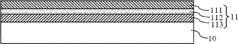
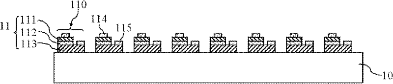
[0034] The direction discussed in the present invention is a method of wafer level packaging. In order to provide a thorough understanding of the present invention, detailed steps and components thereof will be set forth in the following description. Obviously, the practice of the present invention is not limited to the specific details familiar to those skilled in the art of semiconductor package construction. On the other hand, well-known components or steps are not described in detail in order to avoid unnecessarily limiting the invention. The preferred embodiments of the present invention will be described in detail as follows, but in addition to these detailed descriptions, the present invention can also be widely implemented in other embodiments, and the scope of the present invention is not limited, it is based on the following claims .

[0035] Various preferred embodiments and technical content provided by the present invention will be described in detail below in c...


PUM


Abstract

The invention discloses a wafer level package method. A semiconductor component and an encapsulation substrate are combined tightly by using a secondary encapsulation manufacture procedure, so gaps between the wafer and the encapsulation substrate can be reduced, and the combining degree between the wafer and the encapsulation substrate can be improved.

Description

technical field [0001] The invention relates to a packaging method, in particular to a wafer-level packaging method. Background technique [0002] With the increasing demand for semiconductor light-emitting components, the demand for packaging capacity is also increasing. Therefore, many technologies have been revealed to increase the packaging capacity and production efficiency of semiconductor light emitting components, such as wafer level packaging (wafer level package, WLP) technology combined with micro-electromechanical system (micro-electromechanical system, MEMS), using yellow light (photolithography process) and lithography technology (lithography) complete the circuit design and wafer dicing at the wafer level to improve production efficiency and mass production. At the same time, it can also reduce the size of the packaging structure, which is a technology that meets modern needs. [0003] However, there are still many problems to be improved in the wafer-level p...

Claims


Application Information

Patent Timeline
Patent Type & Authority Applications(China)
IPC IPC(8): H01L33/52
CPCH01L33/52H01L33/48H01L2924/181H01L2224/16225H01L2933/0066H01L21/568H01L33/62H01L25/0753H01L2933/005H01L33/54H01L2924/00H01L24/97H01L33/0095H01L2224/97H01L2924/00012
Inventor 林升柏
Owner ZHANJING TECH SHENZHEN
Why Eureka
Try Eureka