

Solar cell element and device
A technology of solar cells and receiving devices, applied in electrical components, circuits, photovoltaic power generation, etc., can solve problems such as reducing conversion efficiency
- Summary
- Abstract
- Description
- Claims
- Application Information
AI Technical Summary
Problems solved by technology
Method used
Image

Examples
Embodiment Construction
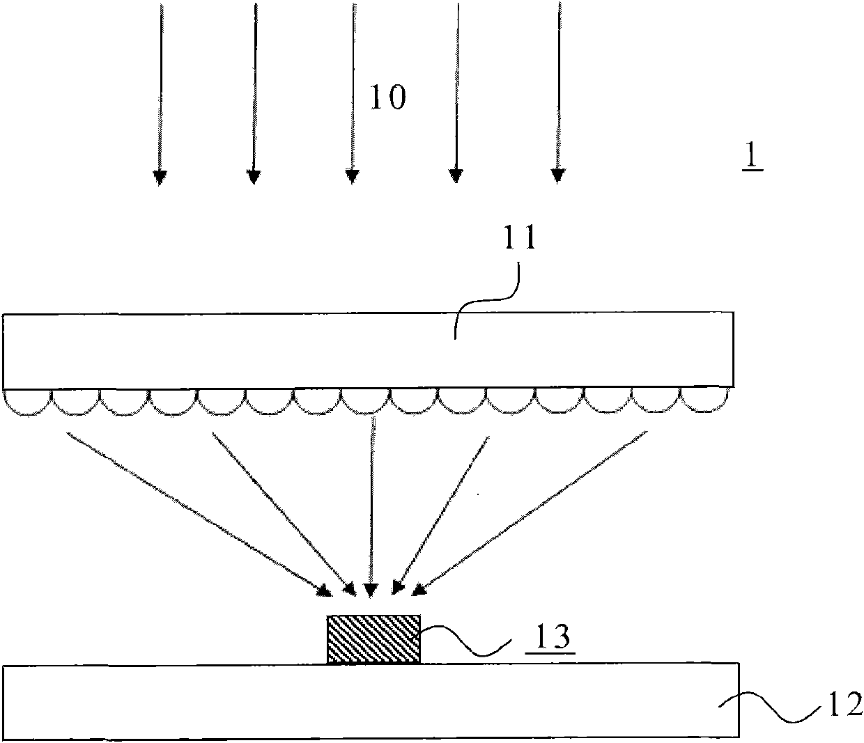
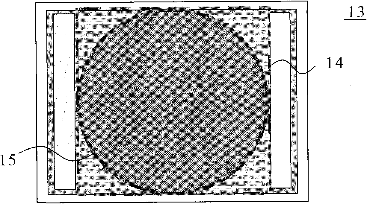
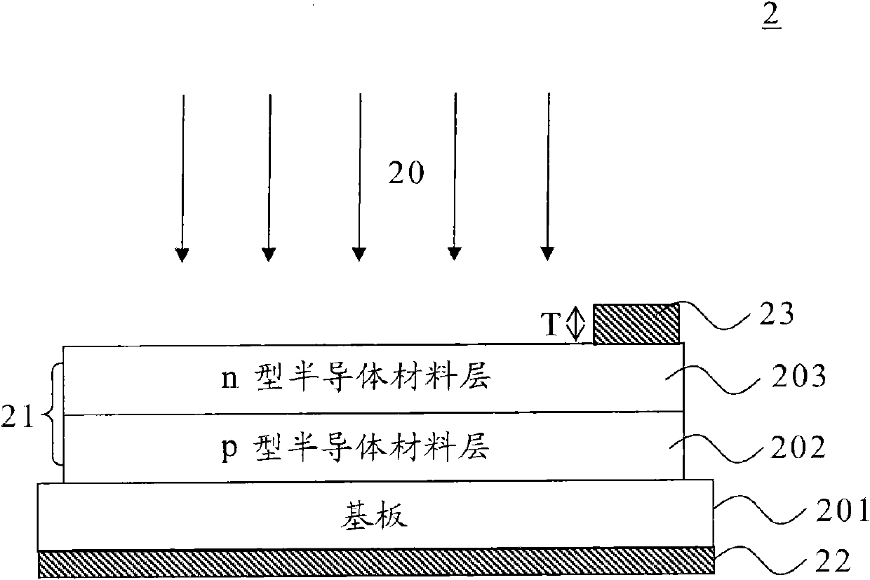
[0062] In order to achieve a more effective application of the light-receiving area of the solar cell receiving device, the present invention proposes a solar cell structure and a solar cell receiving device composed of it. Figure 3A and Figure 3B A cross-section and a top view of a solar cell structure 2 implemented according to the present invention are disclosed. in, Figure 3A for along Figure 3B Transverse section of the A-A' cutting line in .
[0063] Taking the single-junction solar cell structure as an example, the solar cell structure 2 includes a substrate 201, a semiconductor epitaxial structure 21, a p-type semiconductor material layer 202 with a first conductivity characteristic, and an n-type semiconductor material layer with a second conductivity characteristic. The semiconductor material layer 203 is composed. In addition, a first electrode 22 is arranged on one side of the p-type semiconductor material layer 202, connected to the substrate 201 and ele...
PUM
 Abstract
Description
Claims
Application Information