Schottky diode based on non-polar GaN and preparation method thereof

A Schottky diode, non-polar technology, applied in the field of microelectronics, can solve the problems affecting device performance, reducing the density and mobility of two-dimensional electron gas 2DEG, current leakage, etc., to improve device performance and high area utilization efficiency , the effect of large reverse breakdown voltage

Pending Publication Date: 2022-01-21
XIDIAN UNIV
View PDF12 Cites 0 Cited by
  • Summary
  • Abstract
  • Description
  • Claims
  • Application Information

AI Technical Summary

Problems solved by technology

[0004] However, GaN epitaxially grown on different substrates belongs to the lateral structure, because there is a large lattice mismatch between the heterogeneous substrate and GaN, there are different degrees of difference in thermal expansion coefficient, and some non-idealities in the process Factors make the heteroepitaxial GaN material have a high dislocation density, and these dislocation defects have been proved to be the current leakage channel and the main cause of leakage
On the other hand, the lattice mismatch between AlGaN and GaN will also indirectly reduce the 2DEG density and mobility in the heterojunction by affecting the crystal quality, thus affecting the device performance.

Method used


Image

  • Schottky diode based on non-polar GaN and preparation method thereof
  • Schottky diode based on non-polar GaN and preparation method thereof
  • Schottky diode based on non-polar GaN and preparation method thereof

Examples


Embodiment 1

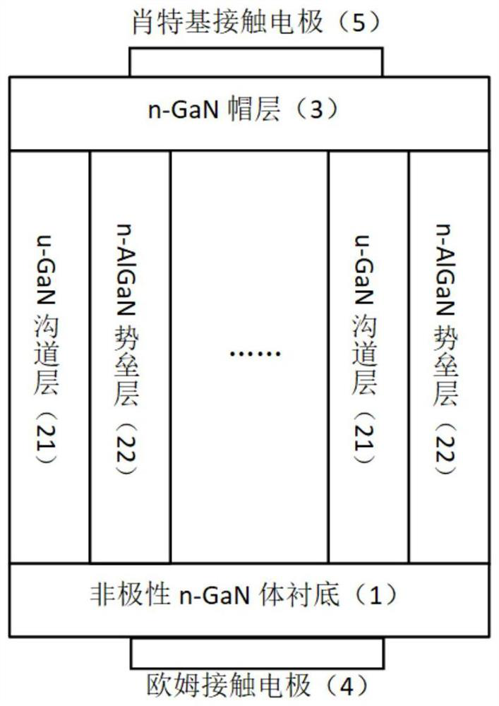
[0035] See figure 1 , figure 1 It is a schematic structural diagram of a non-polar GaN-based Schottky diode provided by an embodiment of the present invention, which includes:

[0036] GaN substrate 1, the vertical multi-channel layer 2 on the GaN substrate 1, the GaN cap layer 3 on the vertical multi-channel layer 2, the ohmic contact electrode 4 on the back side of the GaN substrate 1, and the GaN cap layer Schottky contact electrode 5 on 3; where,

[0037] The GaN substrate 1 is a non-polar n-type GaN bulk substrate;

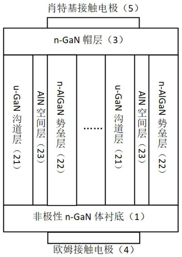
[0038] The vertical multi-channel layer 2 includes several u-GaN channel layers 21 and n-AlGaN barrier layers 22, and the u-GaN channel layers 21 and n-AlGaN barrier layers 22 are arranged at intervals along the horizontal direction to form a Parallel multi-channel structure of substrate 1.

[0039] Since this embodiment uses a bulk material with higher crystal quality as the substrate, the quality of the device is improved.

[0040] Further, all u-GaN c...

Embodiment 2

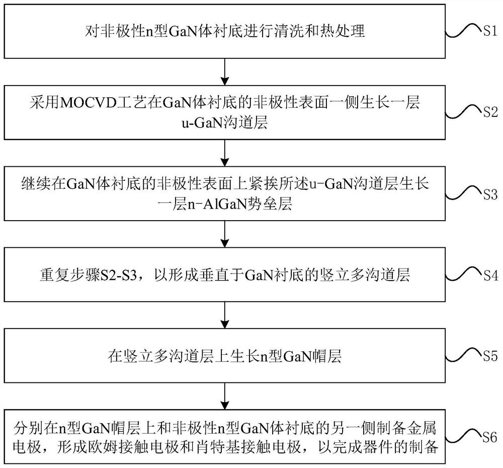
[0055] On the basis of the foregoing first embodiment, this embodiment provides a method for fabricating a non-polar GaN-based Schottky diode. See image 3 , image 3 It is a schematic flowchart of a method for preparing a non-polar GaN-based Schottky diode provided in an embodiment of the present invention, which includes:

[0056] S1: cleaning and heat-treating the non-polar n-type GaN bulk substrate;

[0057] S2: A u-GaN channel layer is grown on the non-polar surface side of the GaN bulk substrate by MOCVD process;

[0058] S3: Continue to grow an n-AlGaN barrier layer on the non-polar surface of the GaN bulk substrate next to the u-GaN channel layer;

[0059] S4: Steps S2-S3 are repeated to form a vertical multi-channel layer perpendicular to the GaN substrate;

[0060] S5: growing an n-type GaN cap layer on the erected multi-channel layer;

[0061] S6: respectively preparing metal electrodes on the n-type GaN cap layer and the other side of the non-polar n-type GaN ...

Embodiment 3

[0094] The following describes the detailed process parameter setting of the present invention by taking the preparation of a non-polar Schottky diode with an Al composition of 20% in the n-AlGaN barrier layer as an example.

[0095] Step 1, cleaning and heat treatment of the substrate:

[0096] 1a) After cleaning the non-polar n-type GaN bulk substrate, put it into the reaction chamber of the metal organic chemical vapor deposition equipment MOCVD, and adjust the vacuum degree of the reaction chamber to be less than 2×10⁻² Torr.

[0097] 1b) Pour hydrogen into the reaction chamber, and when the pressure in the reaction chamber rises to 30 Torr, heat the substrate to 1100° C. to complete the heat treatment of the substrate.

[0098] Step 2, using MOCVD process to perform vertical AlGaN / GaN multi-channel growth on the non-polar n-type GaN bulk substrate, the steps are as follows:

[0099] 2a) Mask the non-polar n-type GaN bulk substrate using a masking process, leaving the reg...


PUM

PropertyMeasurementUnit
thicknessaaaaaaaaaa
thicknessaaaaaaaaaa
thicknessaaaaaaaaaa

Abstract

The invention discloses a Schottky diode based on non-polar GaN and a preparation method thereof. The diode comprises a GaN substrate, a vertical multi-channel layer located on the GaN substrate, a GaN cap layer located on the vertical multi-channel layer, an ohmic contact electrode located on the back surface of the GaN substrate and a Schottky contact electrode located on the GaN cap layer. The GaN substrate is a non-polar n type GaN body substrate; and the vertical multi-channel layer comprises a plurality of u-GaN channel layers and n-AlGaN barrier layers, and the u-GaN channel layers and the n-AlGaN barrier layers are arranged at intervals in the horizontal direction so as to form a parallel multi-channel structure perpendicular to the GaN substrate. The diode improves the crystal quality of the device, inhibits the generation of an electric leakage channel, increases the working current, and can be used for preparing diode devices for high-frequency, low-voltage and large-current rectification.

Description

technical field [0001] The invention belongs to the technical field of microelectronics, and in particular relates to a Schottky diode based on nonpolar GaN and a preparation method thereof. Background technique [0002] Schottky diodes are diodes made using the principle of metal-semiconductor junctions formed by the contact of metals and semiconductors. They are low-power, ultra-high-speed semiconductor devices. Due to its low conduction voltage and no reverse recovery problem, it is widely used in switching power supplies, frequency converters, drives and other circuits. Among them, GaN (gallium nitride)-based Schottky diodes have good development prospects in the power rectifier market due to their advantages such as fast switching speed, high field strength and good thermal characteristics. [0003] In the existing related technologies, GaN power devices are usually prepared by epitaxial AlGaN / GaN heterojunction on silicon carbide or silicon substrates. There is a pol...

Claims


Application Information

Patent Timeline
Patent Type & Authority Applications(China)
IPC IPC(8): H01L29/20H01L29/45H01L29/47H01L29/872H01L21/329
CPCH01L29/0615H01L29/2003H01L29/452H01L29/475H01L29/872H01L29/66143
Inventor 许晟瑞吴前龙陶鸿昌冯兰胜张进成郝跃
Owner XIDIAN UNIV
Why Eureka
Try Eureka