Touch-control module

A touch module and lens technology, which is applied to instruments, electrical digital data processing, and input/output processes of data processing, etc., can solve problems such as affecting positioning accuracy, time-consuming and labor-intensive assembly processes, and optical touch positioning errors, etc. To achieve the effect of reducing the alignment tolerance and assembly tolerance, solving the time-consuming and labor-intensive assembly process, and solving the complex wiring design

Inactive Publication Date: 2011-10-05
AU OPTRONICS CORP
View PDF2 Cites 6 Cited by
  • Summary
  • Abstract
  • Description
  • Claims
  • Application Information

AI Technical Summary

Problems solved by technology

[0004] However, since the above-mentioned optical sensing device 10 is usually aligned with the panel device 14 by aligning with human eyes or automatically aligning with the positioning holes on the housing 20 by the assembly machine, it will As a result, alignment tolerances are likely to occur between the optical sensing device 10 and the panel device 14, and assembly tolerances between the housing 20 and the lens 22, the infrared filter 24, the photosensitive chip 26, and the printed circuit board 28 are often caused. It will affect the positioning accuracy of the lens 22 of the optical sensing device 10 relative to the photosensitive angle of the touch surface of the panel device 14, thereby causing the problem of optical touch positioning errors
[0005] In addition, as can be seen from the above, the optical sensing device 10 must use the housing 20 to fix its internal components (ie lens 22, infrared filter 24, photosensitive chip 26, printed circuit board 28), so it will cause The problem of increasing the overall thickness of the optical sensing device 10 is not conducive to the trend of thinning the optical touch module
In addition, since the optical sensing device 10 needs to additionally use the signal transmission line 30 to transmit the optical signal to the array substrate 18, it will also bring about complicated circuit routing connection design and time-consuming and labor-intensive assembly process.

Method used


Image

  • Touch-control module
  • Touch-control module
  • Touch-control module

Examples


Embodiment Construction

[0027] The technical solution of the present invention will be described in detail below in conjunction with the accompanying drawings and specific embodiments to further understand the purpose, solution and effect of the present invention, but it is not intended to limit the scope of protection of the appended claims of the present invention.

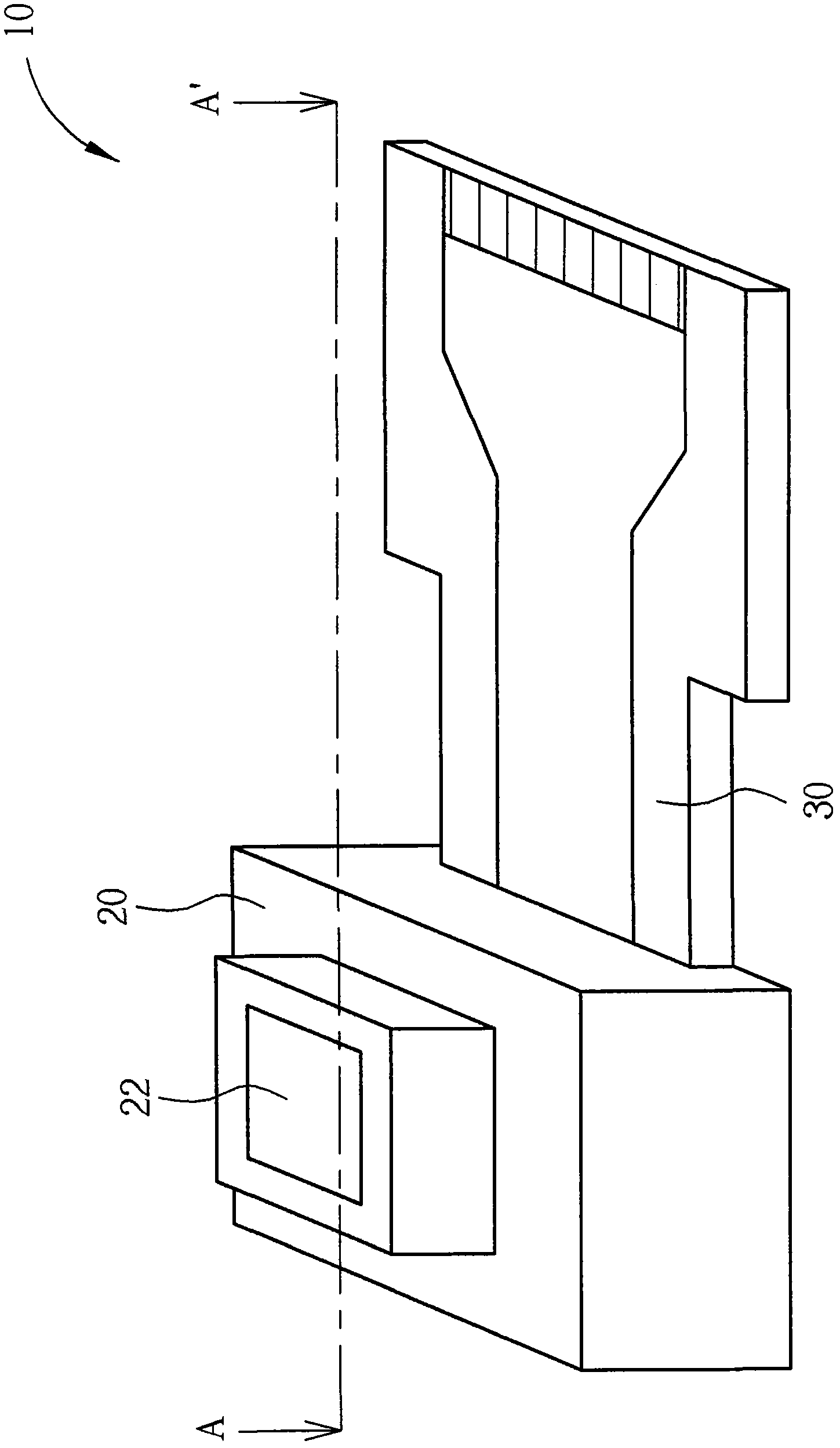
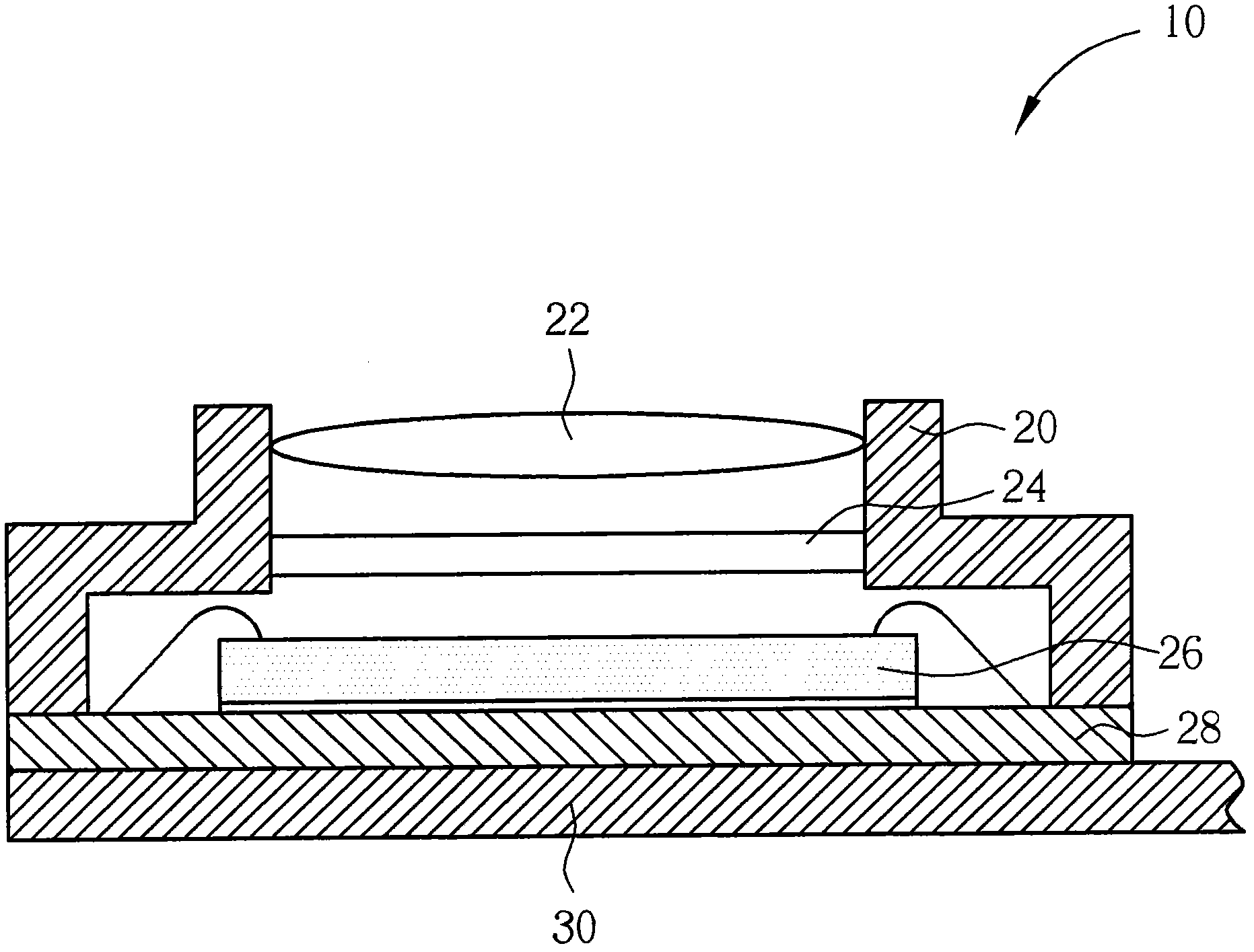
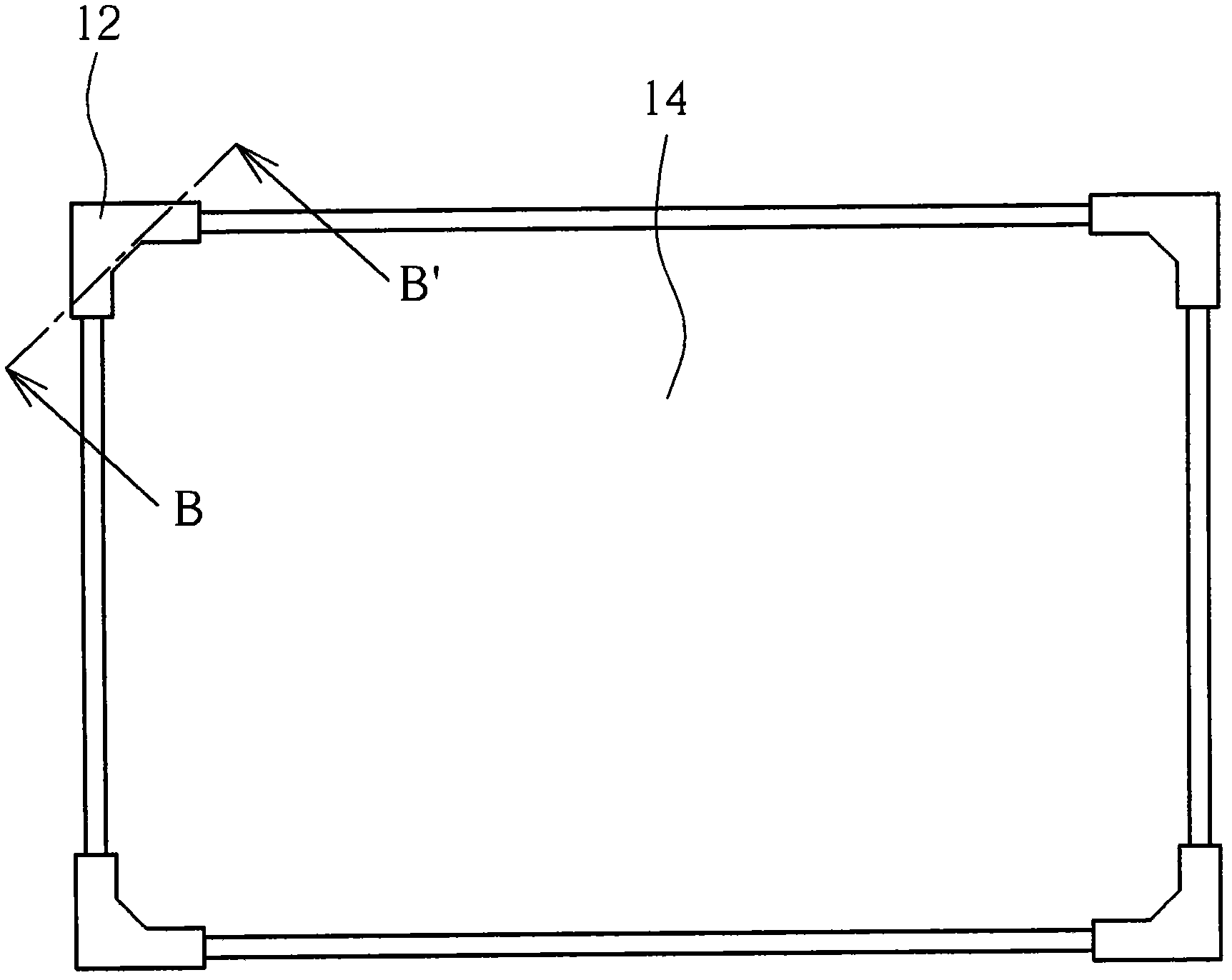
[0028] see Figure 5 as well as Figure 6 , which is a schematic diagram of a touch module 100 proposed according to an embodiment of the present invention, Figure 6 for Figure 5 A schematic cross-sectional view of the touch module 100 along the section line C-C', as shown in Figure 5 as well as Figure 6 As shown, the touch module 100 includes a panel device 102 , a frame 104 , and an optical sensing device 106 . In this embodiment, the panel device 102 is briefly shown as a combination of a display panel 108 and an array substrate 110 . As for the configuration of other related components, it is common in the prior art, so it ...


PUM


Abstract

The invention provides a touch-control module, comprising a panel device, an external frame, and an optical sensing device. The panel device comprises a display panel provided with a touch-control panel and an array substrate. The array substrate is electrically connected with the display panel. The external frame is disposed on the panel device. The optical sensing device is disposed between thepanel device and the external frame, and comprises a circuit wiring, at least a lens, a photosensitive wafer and a reflective lens. The circuit wiring is formed on the array substrate. The lens is disposed between the display panel and the external frame, and used for transmitting sensing light sent via the touch-control panel. The photosensitive wafer is electrically connected with one end of the circuit wiring. The reflective lens is disposed at a position corresponding to the upper part of the photosensitive wafer, and used for reflecting the sensing light sent via the lens to the photosensitive wafer. The touch-control module reduces of structural space required to be occupied by the optical sensing device in the touch-control module, and solves problems of complex wiring of the optical sensing device and time-consuming and labor-consuming of assembly process.

Description

technical field [0001] The present invention relates to a touch module, in particular to a touch module with an optical sensing device in which a lens and a photosensitive chip are respectively arranged on a display panel and an array substrate, and a reflector is arranged above the photosensitive chip. Background technique [0002] Generally speaking, the optical touch module uses the light receiving and blocking principle to detect the relative position of the finger or stylus on the touch surface, and its main configuration is to use an optical sensing device (set on the corresponding touch surface At the position of the left and right top corners), it receives the sensing light transmitted from the touch surface through the light-emitting unit (such as a light-emitting diode), so as to establish an optical touch positioning mechanism on the touch surface, so that When a finger or a stylus touches the touch surface to block the light, the optical sensing device can locate...

Claims


Application Information

Patent Timeline
Patent Type & Authority Applications(China)
IPC IPC(8): G06F3/042
CPCG06F3/0425G06F3/042G06F3/0421G06F3/0428
Inventor 曾堉黄柏辅李常孝
Owner AU OPTRONICS CORP
Why Eureka
Try Eureka