Local positioning cleaning method of wafer surface

A positioning cleaning and wafer technology, applied in cleaning methods and utensils, liquid cleaning methods, chemical instruments and methods, etc., can solve problems such as wafer surface positioning and cleaning, and achieve the effect of precise cleaning methods

Inactive Publication Date: 2011-10-12
叶伟清
View PDF2 Cites 2 Cited by
  • Summary
  • Abstract
  • Description
  • Claims
  • Application Information

AI Technical Summary

Problems solved by technology

[0004] In order to solve the problem of positioning and cleaning the wafer surface, the present invention designs the following technical principles and solutions:

Method used


Image

  • Local positioning cleaning method of wafer surface
  • Local positioning cleaning method of wafer surface
  • Local positioning cleaning method of wafer surface

Examples


Embodiment Construction

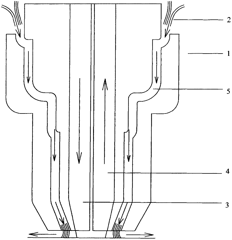
[0017] The present invention specifically adopts the following method to carry out local positioning and cleaning on the surface of the semiconductor wafer:

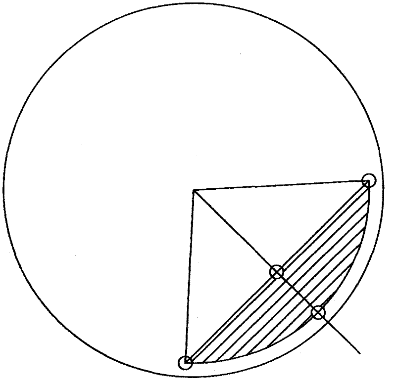
[0018] figure 1 and figure 2 A positioning method for wafer cleaning is shown. Before cleaning, the surface of the wafer is tested to determine the distribution area of ​​pollutants, and then the test results are stored in the computer system; the contaminated wafer to be cleaned is selected, and the wafer is transported to the automatic cleaning device, and in the subsequent cleaning process The data of the contaminated area of ​​the wafer is read out, and the wafer is positioned and cleaned. Pollutants can be tested using conventional techniques such as electrometry. Pollutants include metal pollutants and non-metal ion pollutants, among which metal pollutants include: Li, Be, Na, Mg, Al, K, V, Mn, Fe, Co, Ni, Cu, Zn, Ga, Sr, Y , Ag, Cd, Ba, Pb, Bi, Ce; non-metallic ion pollutants include: F - , Cl - , NO 3 - ...


PUM


Abstract

The invention discloses a local positioning cleaning method of a semiconductor wafer surface. Compared with the conventional whole dipping cleaning technology, the method disclosed by the invention is characterized in that the wafer does not need to be wholly dipped in a large amount of a chemical agent to remove impurities, but is locally subjected to positioning cleaning by using agentia droplets at the tip of a minimal contact. The method has the characteristic that only microlitre-level agentia dose is required in each cleaning process, so as to reach the purpose of removing pollutant on the wafer surface, thus largely reducing the use amount of the cleaning agentia and pure water and reaching the effects of saving energy, reducing emission and reducing manufacturing cost.

Description

technical field [0001] The invention relates to a local positioning cleaning method on the surface of a wafer, in particular to a method for cleaning a designated area on the surface of a wafer. Background technique [0002] With the development and production of ultra-large-scale integrated circuits (ULSI), the line width of silicon wafers (or wafers, wafers, chips) is continuously reduced, and the requirements for manufacturing processes are continuously improved, especially strict specifications for cleanliness Once the inorganic or organic pollutants on the wafer surface exceed the standard, it will seriously affect the quality and yield of ULSI. Therefore, wafer surface cleaning has become a very important and indispensable process in ULSI preparation. Currently, the widely used chemical cleaning method involves immersing the entire wafer in a container for multiple cleanings, which consumes a large amount of chemicals and pure water, which increases manufacturing cost...

Claims


Application Information

Patent Timeline
Patent Type & Authority Applications(China)
IPC IPC(8): H01L21/02B08B3/08
Inventor 叶伟清
Owner 叶伟清
Why Eureka
Try Eureka