Cleaning method of a thin film deposition chamber and method of manufacturing semiconductor device using the cleaning method

a technology of cleaning method and deposition chamber, which is applied in the direction of coating, chemistry apparatus and processes, plasma techniques, etc., can solve the problems of deterioration of achieve the effect of effectively removing the residue and improving the quality of the final product including the thin film

Inactive Publication Date: 2020-04-30
SAMSUNG ELECTRONICS CO LTD
View PDF0 Cites 0 Cited by
  • Summary
  • Abstract
  • Description
  • Claims
  • Application Information

AI Technical Summary

Benefits of technology

[0009]A cleaning method of a thin film deposition chamber in accordance with example embodiments may effectively remove a residue including carbon (C) and/or silicon (Si) by using an oxygen plas...

Problems solved by technology

When the residue remains in the thin film deposition chamber without being completely removed, a thin film may not be uniformly f...

Method used


Image

  • Cleaning method of a thin film deposition chamber and method of manufacturing semiconductor device using the cleaning method
  • Cleaning method of a thin film deposition chamber and method of manufacturing semiconductor device using the cleaning method
  • Cleaning method of a thin film deposition chamber and method of manufacturing semiconductor device using the cleaning method

Examples


Embodiment Construction

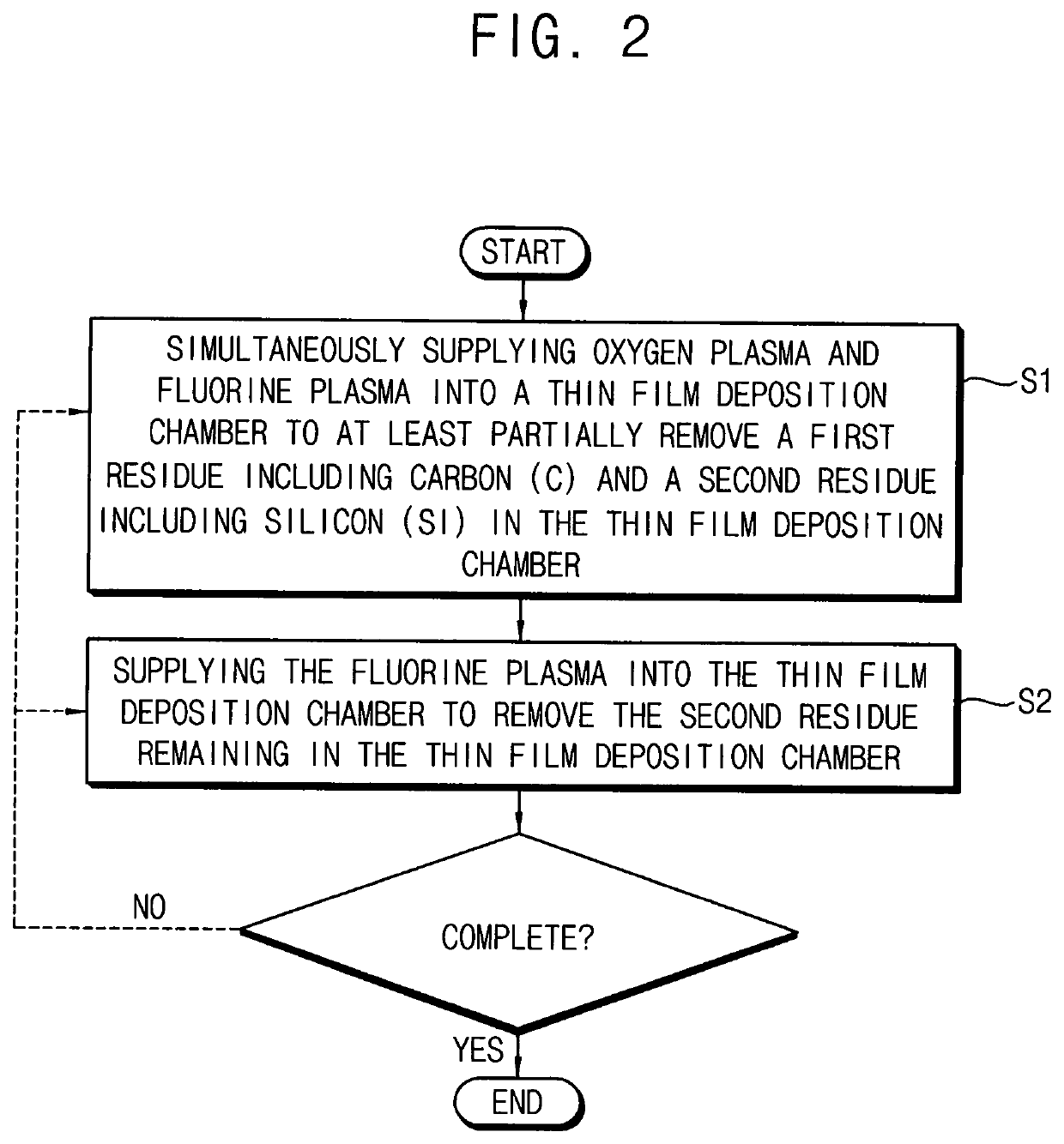
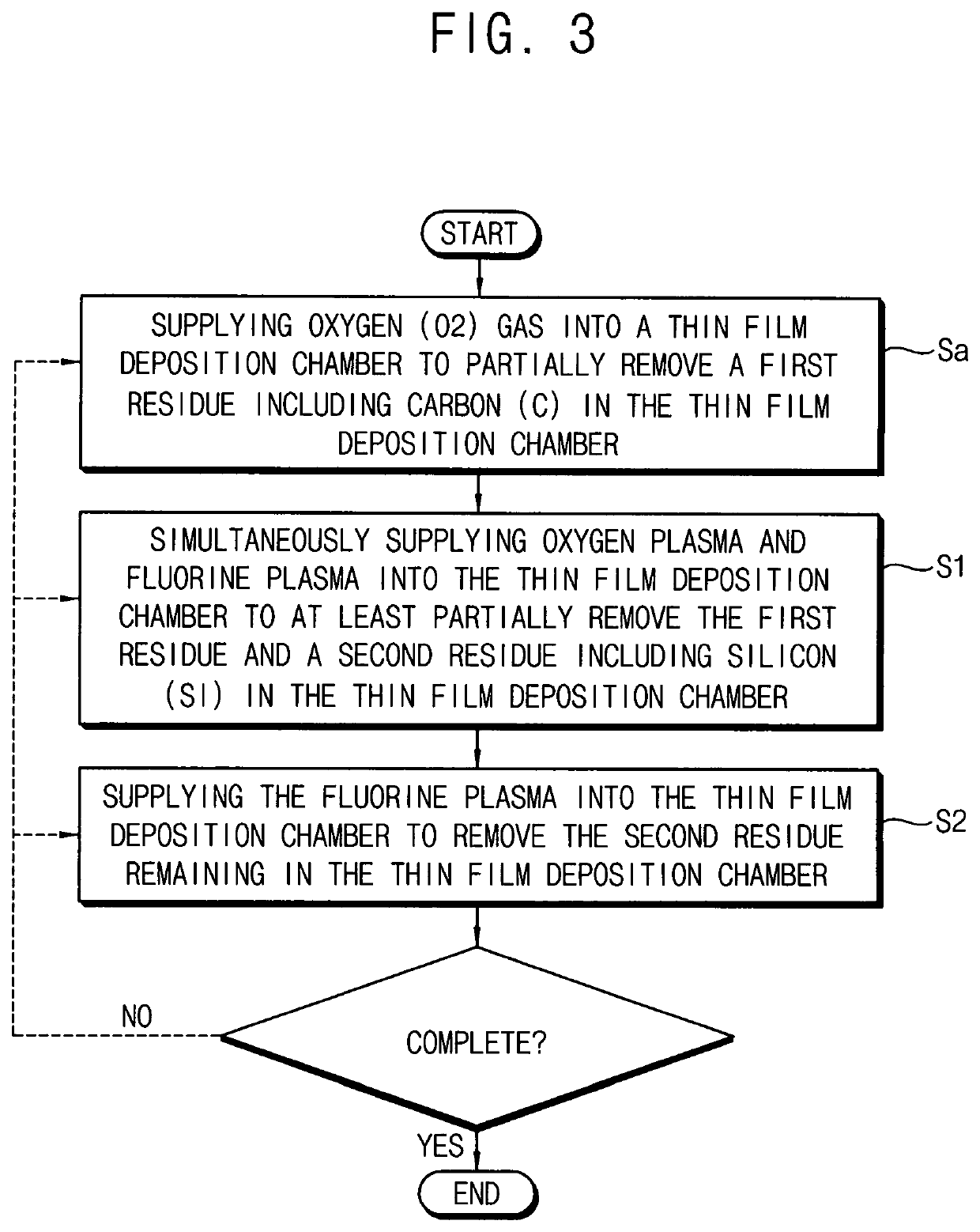
[0012]A cleaning method of a thin film deposition chamber in accordance with example embodiments will be described more fully hereinafter with reference to the accompanying drawings.

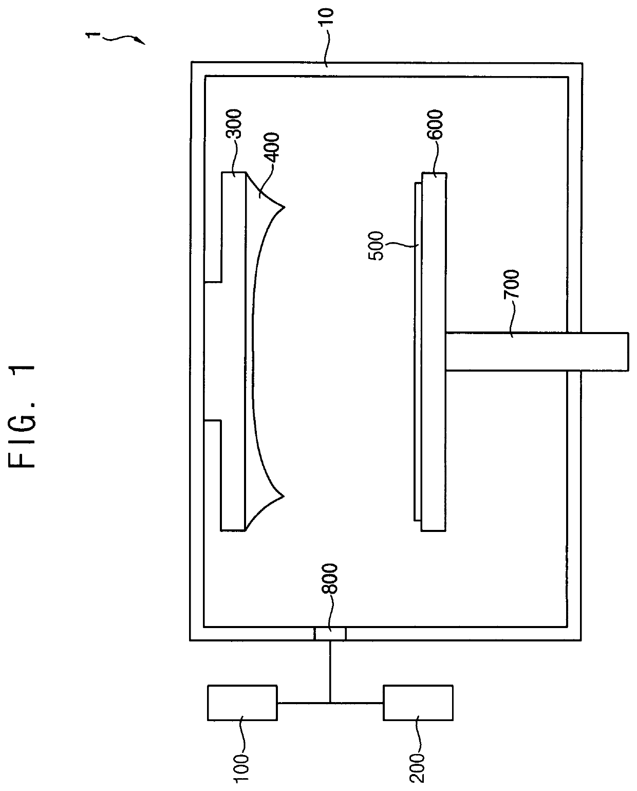
[0013]FIG. 1 is a cross-sectional view illustrating a thin film deposition apparatus in accordance with example embodiments.

[0014]Referring to FIG. 1, a thin film deposition apparatus 1 may include a thin film deposition chamber 10, a gas supply unit 100 and a plasma generating unit 200.

[0015]The thin film deposition chamber 10 may include a shower head 300 spraying gases for forming a thin film, a support unit 600 supporting a substrate 500 on which the thin film may be formed, a driving unit 700 for moving the support unit 600 upwardly / downwardly and / or fastening the support unit 600, and a penetration unit 800 connected to the outside.

[0016]Thin film deposition processes may be performed in the thin film deposition chamber 10, and various by-products may be formed in the chamber 10. Various processing...


PUM


Abstract

A cleaning method of a thin film deposition chamber may include i) simultaneously providing oxygen plasma and fluorine plasma in a thin film deposition chamber to at least partially remove a first residue including carbon (C) and a second residue including silicon (Si) in the thin film deposition chamber, and ii) providing fluorine plasma without oxygen plasma in the thin film deposition chamber to remove the second residue remaining in the thin film deposition chamber.

Description

CROSS-REFERENCE TO RELATED APPLICATION[0001]This application claims priority under 35 USC § 119 to Korean Patent Application No. 10-2018-0129915, filed on Oct. 29, 2018 in the Korean Intellectual Property Office (KIPO), the contents of which are herein incorporated by reference in their entirety.BACKGROUND1. Field[0002]Example embodiments relate to a cleaning method of a thin film deposition chamber and a method of manufacturing a semiconductor device using the cleaning method. More particularly, example embodiments relate to a cleaning method of a thin film deposition chamber with a residue therein.2. Description of the Related Art[0003]A thin film deposition process may be performed in a manufacturing process of a semiconductor device, a display device, etc. The thin film deposition process may be performed using a thin film deposition chamber, however, a residue including carbon (C) and / or silicon (Si) as a reaction by-product may be formed. When the residue remains in the thin f...

Claims


Application Information

Patent Timeline
IPC IPC(8): C23C16/44H01J37/32B08B7/00
CPCB08B7/0035C23C16/4405H01J37/32862B08B7/00H01J37/32449H01L21/67034H01L21/02H05H1/46H01J37/3244
Inventor PARK, MYUNG-JOONKIM, JIN-GWANPARK, MIN-HYEPARK, JOO-MYOUNGAN, SANG-HWAN
Owner SAMSUNG ELECTRONICS CO LTD
Why Eureka
Try Eureka