Semiconductor device

A semiconductor and spacer technology, applied in the direction of semiconductor devices, electrical components, circuits, etc., can solve the problem of reducing the performance of transistors and achieve the effect of reducing the effect of capacitive coupling

Active Publication Date: 2011-10-12
TAIWAN SEMICON MFG CO LTD
View PDF3 Cites 11 Cited by
  • Summary
  • Abstract
  • Description
  • Claims
  • Application Information

AI Technical Summary

Problems solved by technology

This fringe capacitive coupling effect degrades the performance of transistors applied to alternating current (AC)

Method used


Image

  • Semiconductor device
  • Semiconductor device
  • Semiconductor device

Examples


Embodiment Construction

[0031] Hereinafter, each embodiment is described in detail and examples accompanied by accompanying drawings are used as a reference basis of the present invention. In the drawings or descriptions in the specification, the same reference numerals are used for similar or identical parts. And in the drawings, the shapes or thicknesses of the embodiments may be enlarged, and marked for simplicity or convenience. Furthermore, the parts of each element in the drawings will be described separately. It should be noted that the elements not shown or described in the drawings are forms known to those skilled in the art. In addition, specific The examples are only for revealing specific methods used in the present invention, and are not intended to limit the present invention.

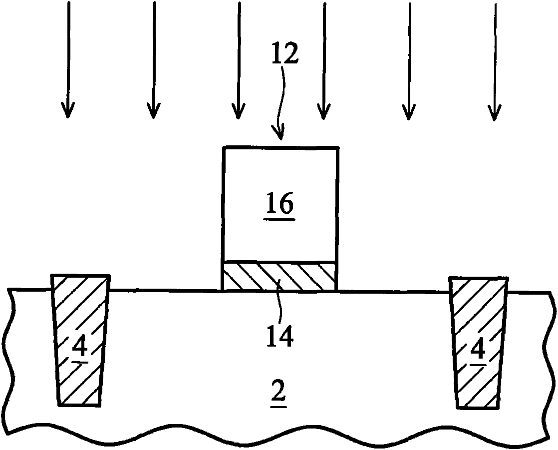
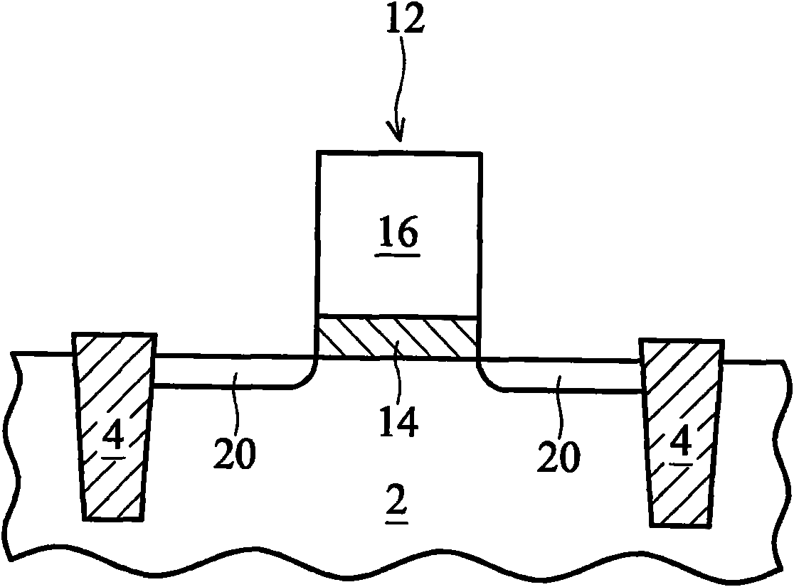
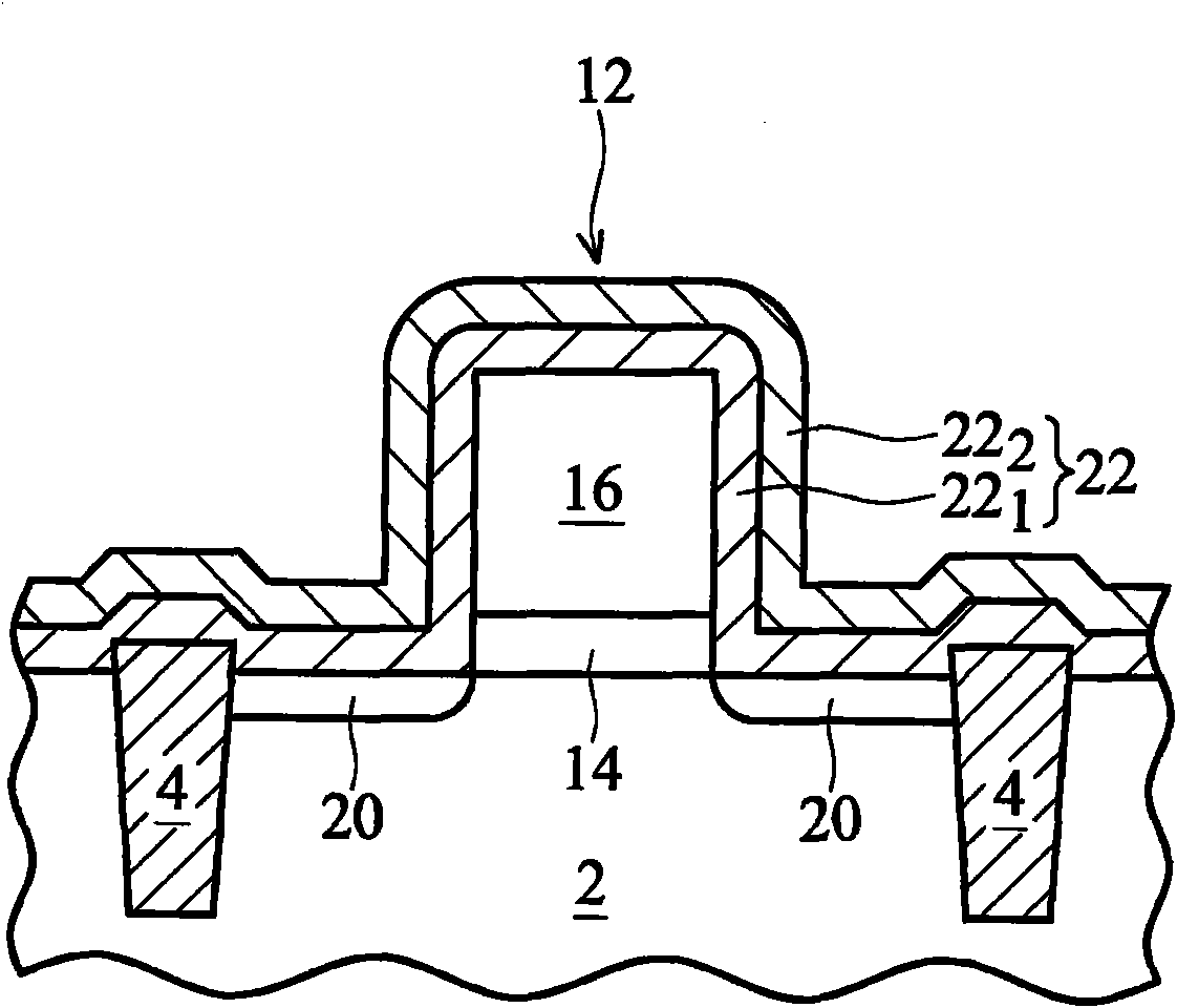
[0032] Please refer to Figure 1 to Figure 8 , the method 200 starts at step 202 , and the step 202 provides a gate stack structure 12 on a substrate 2 . The substrate 2 may comprise bulk silicon. In other e...


PUM


Abstract

The invention provides a semiconductor device, which comprises a substrate having shallow trench isolation and source/drain regions located therein, a gate stack located on the substrate between the source/drain regions, a first gate spacer on the sidewall of the gate stack, and a second gate spacer on the sidewall of the first gate spacer. The dielectric constant of the first gate spacer is smaller than the dielectric constant of the second gate spacer. The dielectric constant of gate spacers, that is the capacitive coupling between the LDD regions and the gate, is reduced.

Description

technical field [0001] The invention relates to a semiconductor device, in particular to a semiconductor device for reducing the capacitive coupling effect between a gate and a lightly doped source / drain (LDD) region. Background technique [0002] The integrated circuit (IC) industry has experienced rapid growth. Technological advances in integrated circuit (IC) materials and design have resulted in each IC generation having smaller and more complex circuits than the previous generation. However, these developments increase the complexity of integrated circuit processes and manufacturing methods, and in order to realize these technological developments, simpler integrated circuit processes and manufacturing methods need to be developed. [0003] During the development of integrated circuits, when the geometric size (that is, the smallest component (or line width) that can be manufactured by a process) shrinks, the functional density (functional density) (that is, the number...

Claims


Application Information

Patent Timeline
Patent Type & Authority Applications(China)
IPC IPC(8): H01L29/78H01L29/08
Inventor 谢博全钟汉邠柯志欣詹博文陶宏远
Owner TAIWAN SEMICON MFG CO LTD
Why Eureka
Try Eureka