
Method for filling redundant metal in manufacturing process of integrated circuit and semiconductor device
A redundant metal and manufacturing process technology, which is applied in the direction of semiconductor devices, semiconductor/solid-state device manufacturing, semiconductor/solid-state device components, etc., can solve the problems of interference, noise energy, consumption, etc., and achieve the reduction of capacitance to ground. Small coupling capacitance, effect of reducing influence
- Summary
- Abstract
- Description
- Claims
- Application Information
AI Technical Summary
Problems solved by technology
Method used
Image

Examples
Embodiment 1
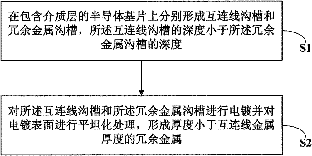
[0032] The method for filling redundant metal in the integrated circuit manufacturing process provided by the embodiment of the present invention aims to reduce the influence of coupling capacitance caused by redundant metal, see figure 1 , the method includes the steps of:
[0033] S1. Form interconnection trenches and redundant metal trenches respectively on the semiconductor substrate including the dielectric layer, and the depth of the redundant metal trenches is smaller than the depth of the interconnection trenches.
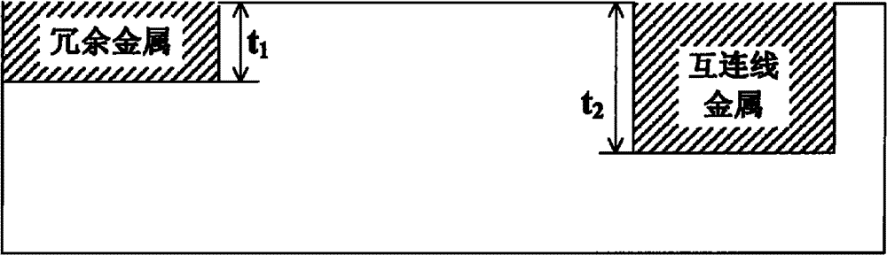
[0034] A semiconductor substrate is provided, and the semiconductor substrate can be a single crystal silicon or a polycrystalline silicon substrate, on which a dielectric layer, namely an oxide layer or an insulating layer is formed. The steps of forming interconnection trenches and forming redundant metal trenches on the dielectric layer are performed separately, and can be realized by processes such as photolithography and etching. see figure 2 , is a...
Embodiment 2
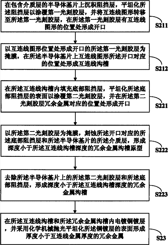
[0039] Embodiment 2 of the present invention is based on Embodiment 1. In Step S1 described in Embodiment 1, interconnect trenches and redundant metal trenches are respectively formed on the semiconductor substrate including the dielectric layer. The redundant metal trenches The depth is less than the depth of the interconnection groove, specifically in this embodiment:
[0040] S21 , forming interconnection line grooves according to the interconnection line pattern on the semiconductor substrate including the dielectric layer.
[0041] Further, see image 3 , the step S21, forming interconnection grooves according to the interconnection pattern on the semiconductor substrate including the dielectric layer, including:
[0042] S211. Deposit a barrier layer 2 on the semiconductor substrate including the dielectric layer 1, planarize the barrier layer 2 to coat the first photoresist layer 3, and transfer the interconnect pattern to the first photoresist layer 3. Form an openin...
Embodiment 3
[0064] see Figure 10 , Embodiment 3 of the present invention provides a semiconductor device aimed at reducing the impact of the coupling capacitance of interconnection lines due to the filling of redundant metal. The semiconductor device includes a multilayer interconnection structure 1, and interconnection structures of different layers The interconnection structure 1 of each layer includes a dielectric layer 3 and an interconnection metal 4 and a redundant metal 5 formed on the dielectric layer, wherein the redundant metal 5 thickness is less than the interconnect metal 4 thickness.
[0065] In the semiconductor device described in the embodiment of the present invention, the thickness of the redundant metal is smaller than the thickness of the metal of the interconnection line, so the distance between the redundant metal and the ground is reduced, and the capacitance to ground caused by the redundant metal is significantly smaller than that of the traditional method, and ...
PUM
 Abstract
Description
Claims
Application Information