Method for manufacturing CMOS (complementary metal-oxide-semiconductor transistor) image sensor

A technology of image sensor and manufacturing method, which is applied in the direction of radiation control devices, etc., can solve problems such as image delay of CMOS image sensors, and achieve the effects of reducing image delay, improving collection efficiency, and reducing quantity

Inactive Publication Date: 2011-10-19
SHANGHAI HUAHONG GRACE SEMICON MFG CORP
View PDF5 Cites 3 Cited by
  • Summary
  • Abstract
  • Description
  • Claims
  • Application Information

AI Technical Summary

Problems solved by technology

[0010] The invention provides a method for manufacturing a CMOS image sensor, which improves the ability of a photodiode to collect photoelectrons, and transfers the collected photoelectrons more effectively, thereby alleviating or even solving the problems of CMOS image sensor image delay and the like

Method used


Image

  • Method for manufacturing CMOS (complementary metal-oxide-semiconductor transistor) image sensor
  • Method for manufacturing CMOS (complementary metal-oxide-semiconductor transistor) image sensor
  • Method for manufacturing CMOS (complementary metal-oxide-semiconductor transistor) image sensor

Examples


Embodiment Construction

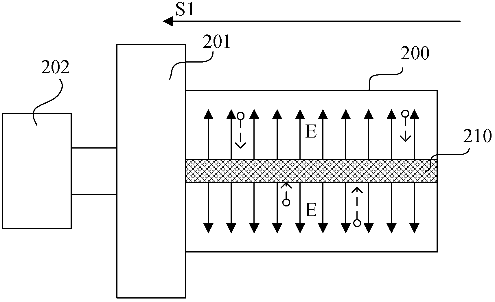
[0024] The CMOS image sensor manufacturing method provided by the present invention, by forming a novel photodiode structure, improves the photodiode’s ability to transfer photoelectrons, increases the diffusion speed of photoelectrons, and reduces the number of photoelectrons stranded in the photodiode, thereby achieving more For effective photoelectron transfer, the image quality, performance and resolution of CMOS image sensors are further improved.

[0025] The manufacturing method of the CMOS image sensor of the present invention will be described in detail below with reference to specific embodiments and accompanying drawings.

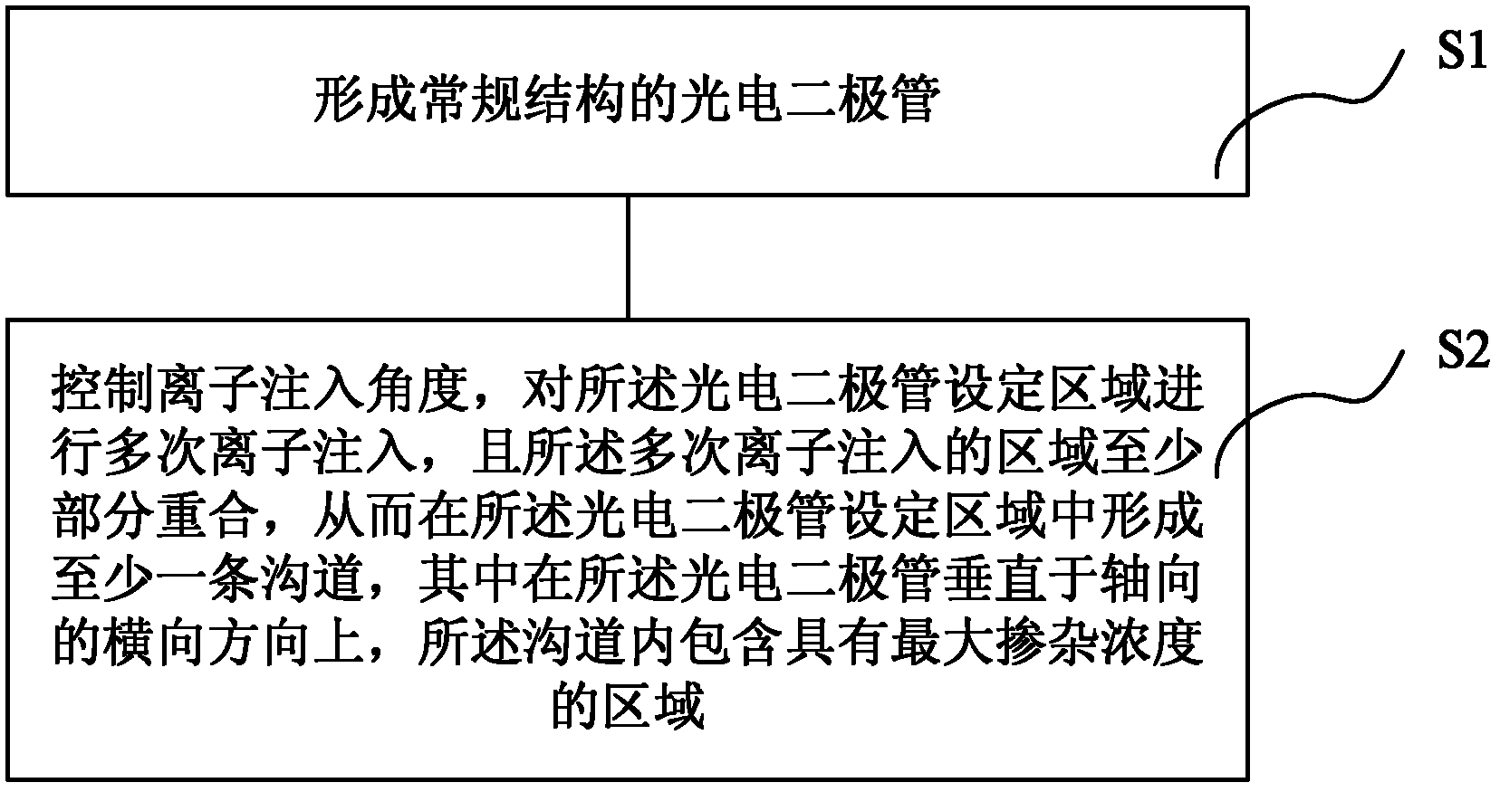
[0026] refer to figure 2 , in one embodiment, the CMOS image sensor manufacturing method of the present invention comprises:

[0027] Step S1, forming a photodiode with a conventional structure;

[0028] Step S2, controlling the ion implantation angle, performing multiple ion implantations on the set area of ​​the photodiode, and the areas of ...


PUM


Abstract

The invention relates to a method for manufacturing a CMOS (complementary metal-oxide-semiconductor transistor) image sensor, wherein the method comprises the steps of: forming a photodiode with a common structure; and controlling an ion injecting angle, carrying out a plurality of times of ion injection on set areas of the photodiode, wherein the areas subjected to the plurality of times of ion injection are partially overlapped, so that at least one trench is formed among the set areas of the photodiode and the trench comprises areas with maximal doping concentration in transverse directions of the photodiode vertical to an axial direction. In the method for manufacturing the CMOS image sensor, the plurality of times of ion injection are carried out on the photodiode and the ion injecting angle is adjusted, thus the trench with the doping concentration greater than of that of the other areas of the photodiode is formed in the photodiode; and the trench comprises the areas with the maximal doping concentration, so that photoelectrons are effectively driven to move, the quantity of the delayed photoelectrons is reduced, the transfer efficiency of the photodiode is improved, and the phenomenon of image delay or information loss is reduced.

Description

technical field [0001] The invention relates to a semiconductor manufacturing process, and in particular to a manufacturing method of a CMOS image sensor. Background technique [0002] The image sensor is an important part of the digital camera. According to different devices, it can be divided into charge-coupled devices (CCD) and complementary metal-oxide semiconductor (CMOS) devices. [0003] Among them, the charge-coupled device (CCD) was developed earlier, and it is often used in high-end technical components of photography and imaging due to its high sensitivity, high resolution and excellent noise control performance. Although CCD has good performance, due to its large size, high power consumption, and incompatibility with the more common standard process in current semiconductor manufacturing technology, its production cost remains high and product compatibility poor. [0004] The CMOS image sensor does not have the inherent defects in the above-mentioned CCD techn...

Claims


Application Information

Patent Timeline
Patent Type & Authority Applications(China)
IPC IPC(8): H01L27/146
Inventor 吴小利张克云
Owner SHANGHAI HUAHONG GRACE SEMICON MFG CORP
Why Eureka
Try Eureka