Pixel circuit, solid-state image pickup device, and camera system

A technology for pixel circuits and imaging devices, applied in the field of solid-state imaging devices, camera systems, and pixel circuits, can solve the problems of insufficiently increasing the amount of potential change, increasing the S/N ratio, and limited dynamic range of FD7 potential, and achieving Ease of charge transfer, effect of increasing charge amount or sensitivity, and improving imaging performance

Active Publication Date: 2011-10-19
SONY SEMICON SOLUTIONS CORP
View PDF7 Cites 9 Cited by
  • Summary
  • Abstract
  • Description
  • Claims
  • Application Information

AI Technical Summary

Problems solved by technology

[0036] However, the dynamic range of the potential of the FD 7 is limited, so there are disadvantages in that the potential change amount ΔVf cannot be sufficiently increased and the S / N ratio cannot be increased

Method used


Image

  • Pixel circuit, solid-state image pickup device, and camera system
  • Pixel circuit, solid-state image pickup device, and camera system
  • Pixel circuit, solid-state image pickup device, and camera system

Examples


no. 1 example

[0084] 1. First Embodiment (First Structural Example of Pixel Circuit)

[0085] 2. Second Embodiment (Second Structural Example of Pixel Circuit)

no. 3 example

[0086] 3. Third Embodiment (Third Structural Example of Pixel Circuit)

no. 4 example

[0087] 4. Fourth Embodiment (Fourth Structural Example of Pixel Circuit)

[0088] 5. Fifth Embodiment (Example of Charge Accumulation Using Deep Depletion State)

[0089] 6. Sixth Embodiment (Example of Charge Accumulation Using Deep Depletion State)

[0090] 7. Seventh Embodiment (Intermediate Reserve Mode)

[0091] 8. Eighth embodiment (intermediate hold mode)

[0092] 9. Ninth Embodiment (Global Shutter Function)

[0093] 10. Tenth embodiment (global shutter function)

[0094] 11. Eleventh Embodiment (Wide Dynamic Range Operation)

[0095] 12. Twelfth Embodiment (Wide Dynamic Range Operation)

[0096] 13. Thirteenth Embodiment (fifth structural example of pixel circuit)

[0097] 14. Fourteenth Embodiment (Sixth Structural Example of Pixel Circuit)

[0098] 15. Fifteenth embodiment (another cross-sectional structure)

[0099] 16. Sixteenth embodiment (another cross-sectional structure)

[0100] 17. Seventeenth embodiment (camera system)

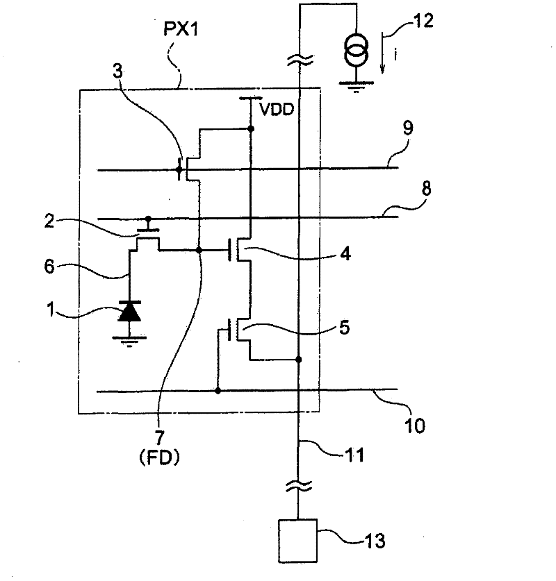
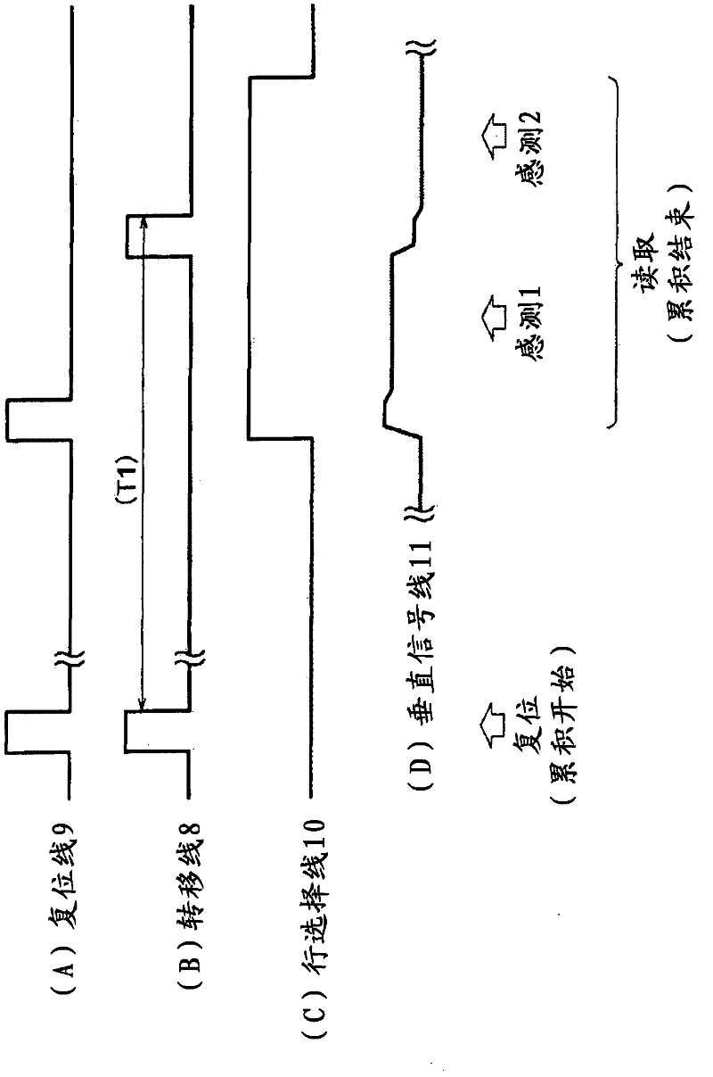
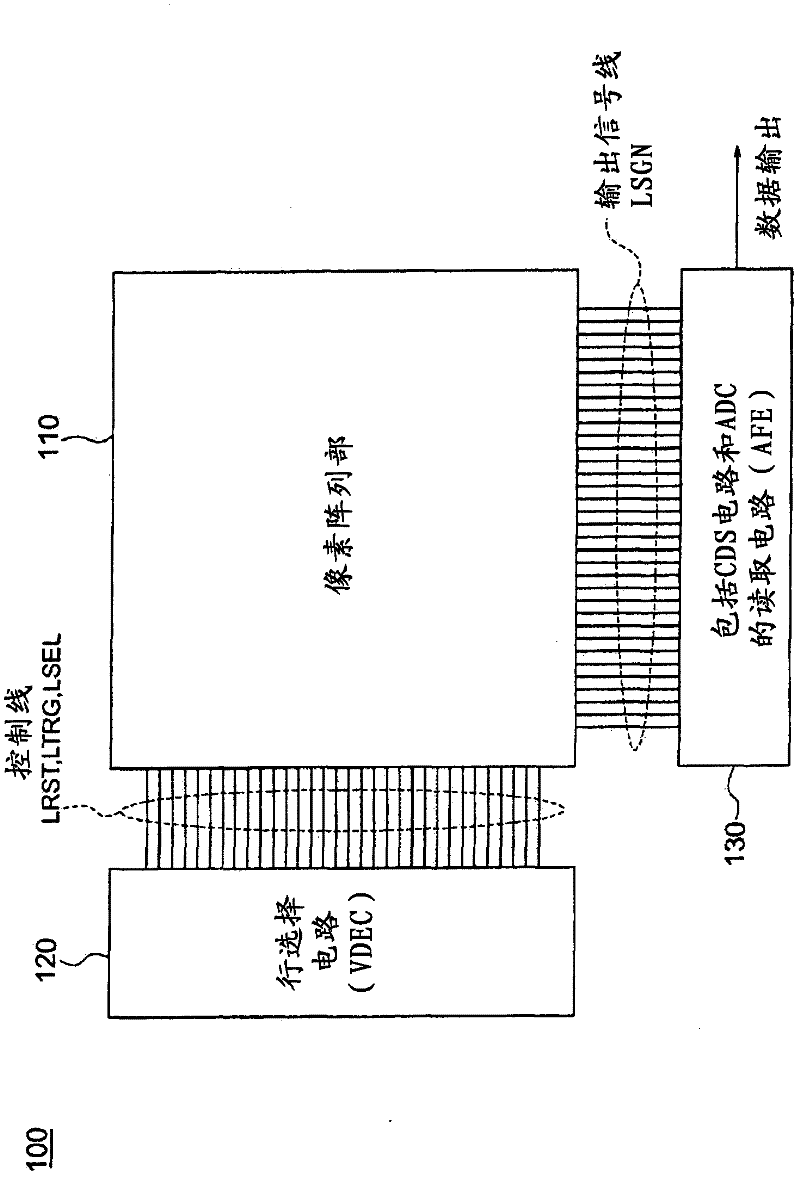
[0101] image 3 is a schema...


PUM


Abstract

A transfer transistor (112) has first, second and third field effect transistors (1121-1123) that are integrally series-connected between a photoelectric conversion element (111) and an amplifier circuit. The first and second field effect transistors are configured such that the gate electrodes of the first and second field effect transistors are collectively driven at the same time. It is further arranged that the threshold voltage of the first field effect transistor be higher than that of the second field effect transistor. As the gate electrodes of the first, second and third field effect transistors are driven in stages, electrons, which are generated by the photoelectric conversion element and transferred through the first field effect transistor, are accumulated in the channel region of the second field effect transistor, and the electrons accumulated in the channel region are transferred to the input of the amplifier circuit via the third field effect transistor.

Description

technical field [0001] The present invention relates to a pixel circuit represented by a CMOS image sensor, a solid-state imaging device and a camera system. Background technique [0002] In recent years, CMOS imagers for digital cameras, camcorders, security cameras, etc. have been widely used and the market has expanded. [0003] A CMOS imager converts light incident on each pixel into electrons through a photodiode as a photoelectric conversion element, accumulates the electrons for a fixed period of time, digitizes a signal reflecting the amount of charge it has accumulated, and outputs the digitized signal to the outside. [0004] figure 1 is a schematic diagram showing an example of a pixel circuit including four transistors in one unit pixel. [0005] One unit of pixel circuit PX1 has photodiode 1 , transfer transistor 2 , reset transistor 3 , amplification circuit 4 , row selection transistor 5 , accumulation node 6 , and floating diffusion (FD, floating diffusion...

Claims


Application Information

Patent Timeline
Patent Type & Authority Applications(China)
IPC IPC(8): H04N5/3745H04N5/359H01L27/146H04N5/355
CPCH01L27/14609H04N25/59H04N25/77
Inventor 西原利幸
Owner SONY SEMICON SOLUTIONS CORP
Why Eureka
Try Eureka