Integrated circuit and method of manufacturing same

A technology of integrated circuits and manufacturing methods, which is applied in the direction of circuits, semiconductor/solid-state device manufacturing, and electrical components, and can solve problems such as polysilicon resistance damage, dents, polysilicon resistance resistance and set value deviations, etc.

Active Publication Date: 2011-11-09
TAIWAN SEMICON MFG CO LTD
View PDF3 Cites 17 Cited by
  • Summary
  • Abstract
  • Description
  • Claims
  • Application Information

AI Technical Summary

Problems solved by technology

However, the formed polysilicon resistors will be damaged and sunken due to the etching process, resulting in deviations between the resistance value of the polysilicon resistors and the set value and other problems

Method used


Image

  • Integrated circuit and method of manufacturing same
  • Integrated circuit and method of manufacturing same
  • Integrated circuit and method of manufacturing same

Examples


Embodiment Construction

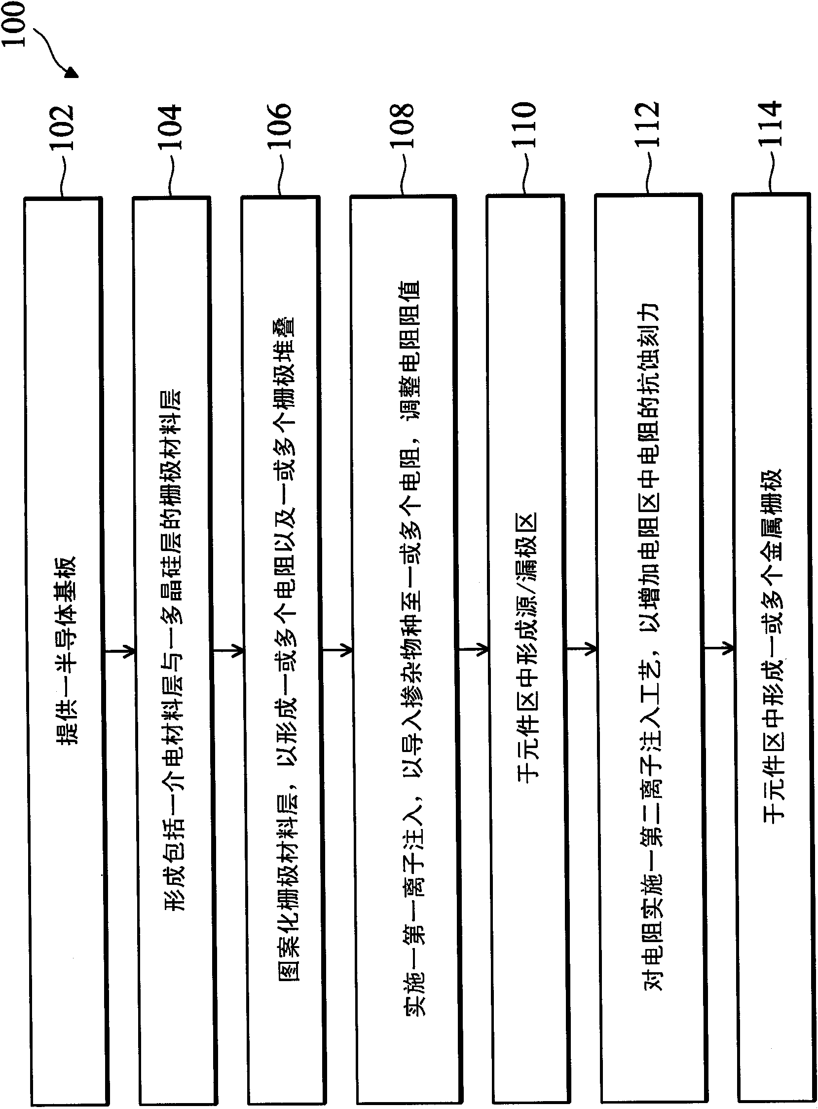
[0045] figure 1 It is a flowchart of a semiconductor device manufacturing method 100 according to an embodiment. According to different aspects of the present invention, the semiconductor device includes a metal gate stack and a polysilicon resistor. Figure 2 to Figure 9 A cross-sectional view of a semiconductor structure 200 at different process stages according to one or more embodiments. The semiconductor structure 200 and its method of fabrication 100 are fully described in Figure 1 to Figure 11 .

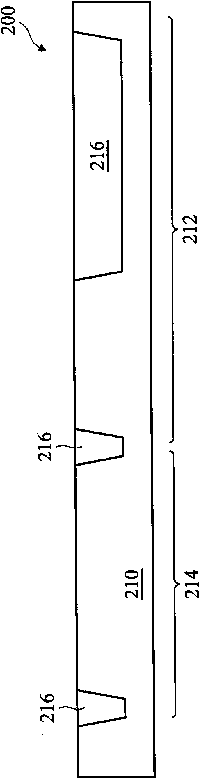
[0046] see figure 1 and figure 2 , the method 100 starts at step 102 , providing a semiconductor substrate 210 . The semiconductor substrate 210 includes silicon. The semiconductor substrate 210 optionally includes germanium, silicon germanium or other suitable semiconductor materials. The semiconductor substrate 210 also includes various isolation structures, such as shallow trench isolation (STI) formed in the substrate to separate various devices. The semiconducto...


PUM


Abstract

The invention provides an integrated circuit and a method of manufacturing the same. The method includes forming a polysilicon layer on a substrate; and patterning the polysilicon layer to form a polysilicon resistor and a polysilicon gate. A first ion implantation is performed on the polysilicon resistor to adjust electric resistance of the polysilicon resistor. A second ion implantation is performed on a top portion of the polysilicon resistor such that the top portion of the polysilicon resistor has an enhanced etch resistance. An etch process is then used to remove the polysilicon gate while the polysilicon resistor is protected by the top portion. The invention could conquer the deviation of the resistance of the polysisilcon resistor from the designed target and other problems.

Description

technical field [0001] The invention relates to an integrated circuit, in particular to an integrated circuit with a novel ion implantation method and a manufacturing method thereof. Background technique [0002] Polysilicon resistors have been frequently used in conventional integrated circuit (IC) designs. Likewise, due to technology node scaling, high-k dielectric materials and metals are often considered as a gate stack of a semiconductor device such as a metal oxide semiconductor field effect transistor (MOSFET). However, when combining polysilicon resistors with the metal gates of MOSFETs into a single integrated circuit (IC) die, different integration issues arise. Solutions include using a dummy gate when forming a polysilicon resistor. Afterwards, a gate-last process, such as an etching process, may be performed to remove the dummy gate. However, the formed polysilicon resistors will be damaged and recessed due to the etching process, resulting in deviations betw...

Claims


Application Information

Patent Timeline
Patent Type & Authority Applications(China)
IPC IPC(8): H01L21/822H01L21/266H01L27/06
CPCH01L29/4966H01L21/28088H01L29/66545H01L29/517H01L29/7833H01L27/0629H01L21/26513H01L29/7848H01L29/6659H01L21/2658
Inventor 李达元叶明熙
Owner TAIWAN SEMICON MFG CO LTD
Why Eureka
Try Eureka