Chip with thickened metal layer of press welding block and manufacturing method for chip

A technology of metal layer and pressure soldering block, which is applied in semiconductor/solid-state device manufacturing, electrical components, electric solid-state devices, etc., can solve problems such as not reaching the ideal level, and achieve the effect of meeting the thickness requirements

Inactive Publication Date: 2011-11-09
PEKING UNIV FOUNDER GRP CO LTD +1
View PDF6 Cites 7 Cited by
  • Summary
  • Abstract
  • Description
  • Claims
  • Application Information

AI Technical Summary

Problems solved by technology
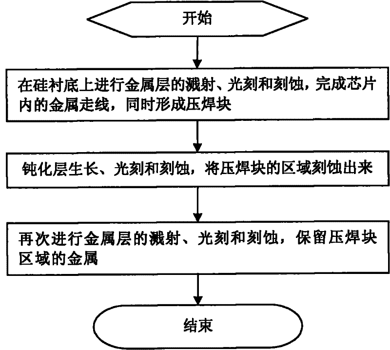
However, this improvement has not reached the desired level

Method used


Image

  • Chip with thickened metal layer of press welding block and manufacturing method for chip
  • Chip with thickened metal layer of press welding block and manufacturing method for chip
  • Chip with thickened metal layer of press welding block and manufacturing method for chip

Examples


Embodiment 1

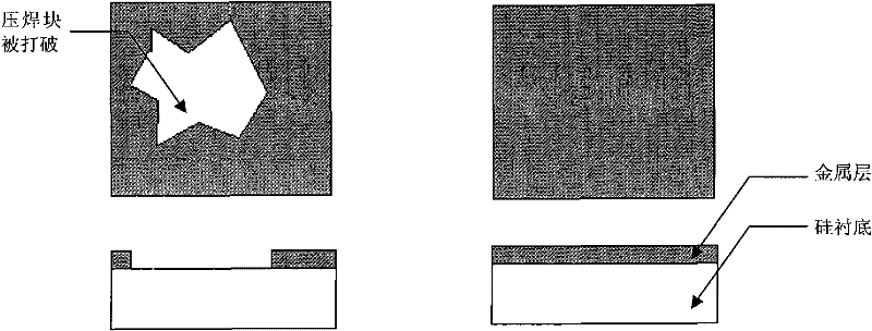
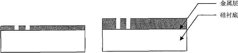
[0024] The structure of the chip in this embodiment is as follows Figure 7 shown. Copper wires are used for bonding during chip packaging, and the diameter of the copper wires used in this embodiment is 0.8 mil. During chip fabrication, the thickness of the metal layer of the pad is 1.0 μm. Tests have shown that if the thickness is less than 1.0 μm, the pads are easily pierced when a copper wire with a diameter of 0.8 mil is used for bonding. The composition of the pressure soldering block is an alloy of Al (aluminum), Si (silicon) and Cu (copper), wherein Al accounts for about 98%.

Embodiment 2

[0026] The structure of the chip in this embodiment is as follows Figure 7 shown. Copper wires are used for bonding during chip packaging, and the diameter of the copper wires used in this embodiment is 1.0 mil. During chip manufacturing, the thickness of the metal layer of the pad is 1.5 μm. Tests have shown that if the thickness is less than 1.5 μm, the pads are easily pierced when a copper wire with a diameter of 1.0 mil is used for bonding. The composition of the bonding block is the same as in Example 1.

Embodiment 3

[0028] The structure of the chip in this embodiment is as follows Figure 7 shown. Copper wires are used for bonding during chip packaging, and the diameter of the copper wires used in this embodiment is 1.2mil. During chip fabrication, the thickness of the metal layer of the pad is 2.0 μm. Tests have shown that if the thickness is less than 2.0 μm, the pads are easily pierced when a copper wire with a diameter of 1.2 mil is used for bonding. The composition of the bonding block is the same as in Example 1.


PUM

PropertyMeasurementUnit
Thicknessaaaaaaaaaa
Thicknessaaaaaaaaaa
Thicknessaaaaaaaaaa

Abstract

The invention discloses a chip with a thickened metal layer of a press welding block and a manufacturing method for the chip and belongs to the technical field of semiconductor chip manufacturing. The chip comprises a silicon substrate, a metal layer on the silicon substrate, a passivation layer on the metal layer and the press welding block on the metal layer, wherein the thickness of the metal layer of the press welding block is greater than that of the metal layer of a metal wire. The manufacturing method for the chip comprises the following steps of: sputtering, photoetching and etching the metal layer on the surface of the silicon substrate according to the function of the chip so as to form the metal wire and the press welding block in the chip; growing, photoetching and etching the passivation layer and etching a press welding block region; and sputtering, photoetching and etching the metal layer again on the surface of the passivation layer and retaining the metal in the press welding block region. During manufacturing of the chip, an effect of independently thickening the press welding block inside the chip is achieved and the requirement of a chip package factory on the thickness of the metal layer of the press welding block inside the chip during routing by using a copper wire is met.

Description

technical field [0001] The invention belongs to the technical field of semiconductor chip manufacturing, and in particular relates to a chip with a thickened metal layer of a pad and a manufacturing method thereof. Background technique [0002] The development trend of the chip packaging process is to gradually use copper wires as bonding wires instead of gold wires and aluminum wires. Mainly because copper wire has a series of advantages such as low resistivity, high thermal conductivity, and low price. However, compared with gold wires and aluminum wires, copper wires have higher hardness and are easy to oxidize. When bonding wires, it is easy to break the chip pads (such as figure 1 As shown), so when copper wire is used for packaging and wiring, the requirements for the thickness of the metal layer of the chip bonding pad are also higher, and the thicker the copper wire, the thicker the requirement for the thickness of the metal layer of the bonding pad. [0003] In th...

Claims


Application Information

Patent Timeline
IPC IPC(8): H01L23/485H01L21/60
CPCH01L2224/85H01L24/85H01L2924/01013H01L2924/10253H01L24/05H01L2224/45147H01L2924/01014H01L2924/01029H01L2924/00014H01L2224/45124H01L2224/45015H01L2924/01033H01L24/45H01L2224/45H01L2924/20751H01L2924/20752H01L2924/20753H01L2924/20754H01L2924/20755H01L2924/20756H01L2924/20757H01L2924/20758H01L2924/20759H01L2924/2076H01L2224/48H01L2924/00H01L2924/00012
Inventor 马万里赵文魁
Owner PEKING UNIV FOUNDER GRP CO LTD
Why Eureka
Try Eureka