Chip on film (COF) and COF carrier tape

A carrier and line edge technology, applied in the field of COF, can solve the problems of occupying carrier tape and wasting materials.

Inactive Publication Date: 2011-11-09
SHENZHEN CHINA STAR OPTOELECTRONICS TECH CO LTD
View PDF2 Cites 2 Cited by
  • Summary
  • Abstract
  • Description
  • Claims
  • Application Information

AI Technical Summary

Problems solved by technology

The COF100 in the COF carrier tape has a rectangular structure, and the area of ​​the shaded part 101 is useless, but it also occupies a part of the area of ​​the carrier tape, and a large amount of material will be wasted during mass production

Method used


Image

  • Chip on film (COF) and COF carrier tape
  • Chip on film (COF) and COF carrier tape
  • Chip on film (COF) and COF carrier tape

Examples


Embodiment Construction

[0023] It should be understood that the specific embodiments described here are only used to explain the present invention, not to limit the present invention.

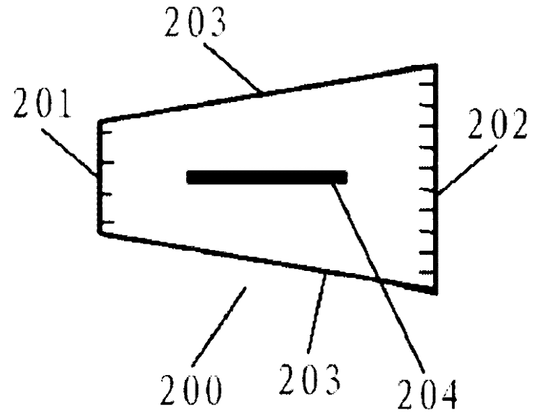
[0024] refer to image 3 , image 3 It is a structural schematic diagram of the first embodiment of the COF200 of the present invention. The shape of the COF 200 is a trapezoid formed by two opposite sides parallel to each other and two non-parallel sides 203. The COF 200 in this embodiment has an isosceles trapezoidal structure, and the two routing sides are respectively the upper base 201 and the bottom edge 202. One short trace side of COF200, that is, the upper bottom 201 is provided with several wires that can be connected to an external PCB, and the other long trace, that is, the lower bottom 202 is provided with several wires that can be connected to an external panel, and the upper bottom 201 is provided with The number of wires is less, and the lower bottom 202 has more wires. In this embodiment, the upper...


PUM


Abstract

The invention discloses a chip on film (COF) carrier tape. The COF carrier tape comprises a COF tape consisting of a plurality of COFs which are connected sequentially, and a carrier connected with the COF tape, wherein each COF has a trapezoidal shape consisting of two parallel routing edges and two non-parallel side edges; between two adjacent COFs, the long routing edge of one COF and the short routing edge of the other COF are connected with each other and positioned on the same straight line; and the other short routing edge and the other long routing edge of the two COFs are connected with each other and positioned on the same straight line. The invention provides the COF which has the trapezoidal shape consisting of two parallel routing edges and two non-parallel side edges. The COF saves materials; and in a carrier tape type semiconductor device, the number of COFs can be increased on the carrier tape with a specified length and the cost can be reduced greatly.

Description

technical field [0001] The present invention relates to COF (Chip On Film, chip-on-film), in particular to a COF and a COF carrier tape. Background technique [0002] COF carrier tape is to bond and install semiconductor components on a long carrier tape. COF uses a soft additional circuit board as a packaged chip carrier to bond the chip with a flexible substrate circuit, or simply refers to the soft additional circuit board of an unpackaged chip. . Such as figure 1 As shown, COF is the chip (source driver IC or gate driver IC, etc., such as figure 1 The shaded part in black) is bonded and mounted on a flexible wiring substrate on which a wiring pattern is formed. The wiring pattern of COF usually consists of inner leads connected to the electrodes of the chip and outer leads connected to external circuits. Usually, in the driving circuit of the LCD TV, the wiring at one end of the COF connected to the PCB (Printed Circuit Board, printed circuit board) is relatively spa...

Claims


Application Information

Patent Timeline
IPC IPC(8): H01L23/498
CPCH01L23/4985H01L23/498H01L2924/15162H01L2924/0002H01L2924/00
Inventor 林柏伸廖良展张勇
Owner SHENZHEN CHINA STAR OPTOELECTRONICS TECH CO LTD
Why Eureka
Try Eureka