Active pixel cell and method of preparing the same on substrate

A technology of pixel units and substrates, applied in electrical components, image communication, color TV components, etc., to achieve the effect of reducing the number of white units and reducing the leakage current of dark states

Active Publication Date: 2011-11-09
TAIWAN SEMICON MFG CO LTD
View PDF4 Cites 5 Cited by
  • Summary
  • Abstract
  • Description
  • Claims
  • Application Information

AI Technical Summary

Problems solved by technology

As a result, the effect of dark state l

Method used


Image

  • Active pixel cell and method of preparing the same on substrate
  • Active pixel cell and method of preparing the same on substrate
  • Active pixel cell and method of preparing the same on substrate

Examples


Embodiment Construction

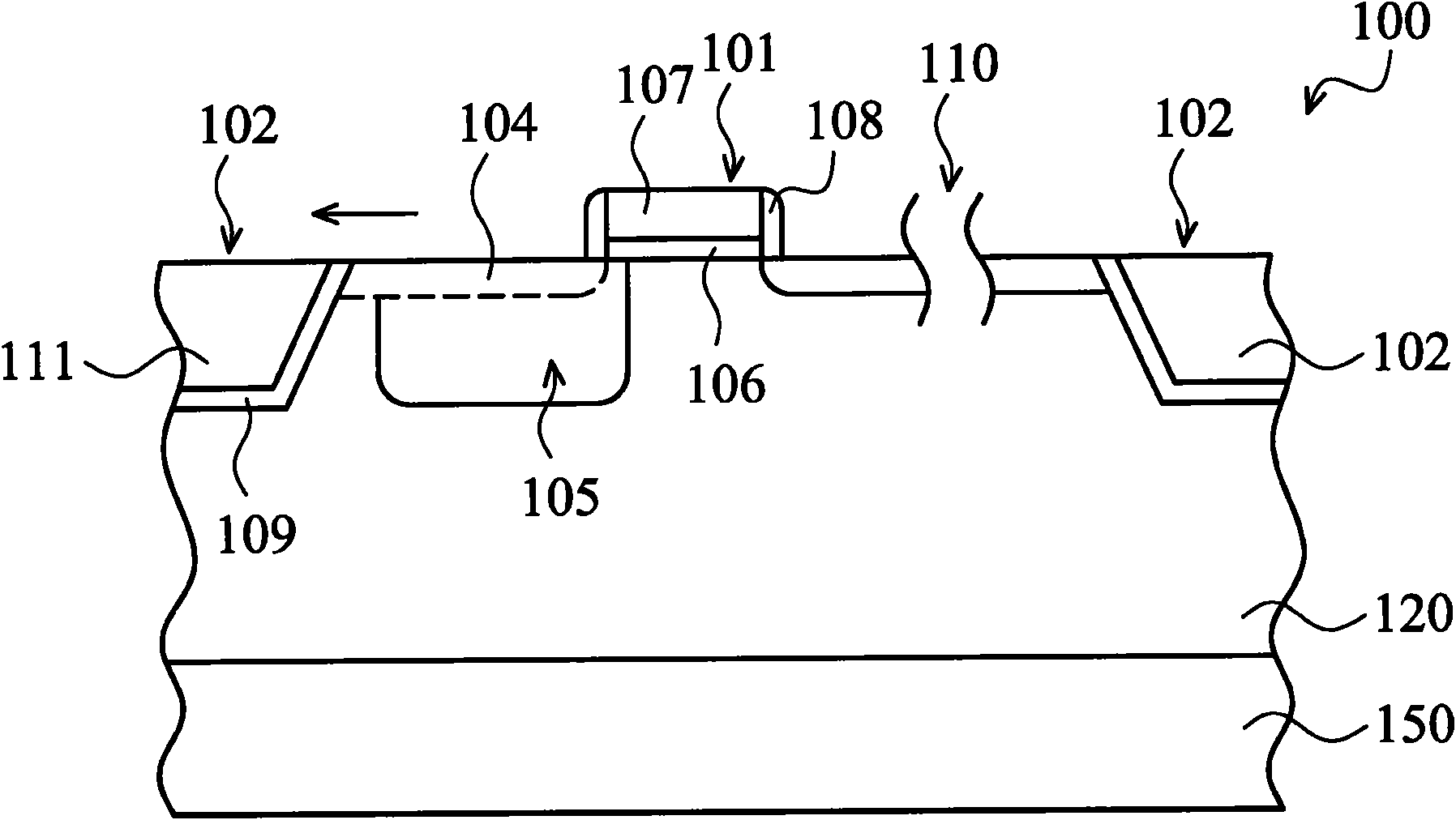
[0055] figure 1 A cross-sectional view of an active pixel unit 100 according to various embodiments of the invention is shown. Here, the active pixel unit 100 is a complementary metal oxide semiconductor image sensor (CMOS image sensor, referred to as CIS hereinafter), which has a photodiode 105 , a transistor 101 and a plurality of isolation structures 102 . Details of a portion 110 of the active pixel unit 100 are not shown here. The portion 110 may include one or more transistors, diffusion regions, and additional isolation structures. The active pixel unit 100 can be any type of pixel unit, such as a five-transistor (5T), four-transistor (4T), three-transistor (3T) or one-transistor (1T) pixel unit. Such transistors as the four transistors for a 4T pixel cell are used to control the operation of the active pixel cell 100 within the active pixel cell 100 . In some embodiments, the transistor 101 is an N-type metal oxide semiconductor transistor (NMOS), and the photodiode...


PUM


Abstract

The invention provides an active pixel cell structure and a method of preparing the same on a substrate, so as to enable reduction of dark current and white cell counts for active pixel cells. The process of preparing active pixel cell structures introduces stress on the substrate, which could lead to increased dark current and white cell counts of active pixel cells. By depositing a stress layeras part of a pre-metal dielectric layer with a stress that counters the stress induced, both the dark current and the white cell counts can be reduced. If the transistors of the active pixel cells are NMOS, the carrier mobility can also be increased by a tensile stress layer. Raman Spectroscopy can be used to measure the stress exerted on the substrate prior to the deposition of the stress layer.The invention can reduce the dark current and white cell counts for the active pixel cells.

Description

technical field [0001] The present invention relates to a complementary metal-oxide semiconductor (complementary metal-oxide semiconductor, CMOS) image sensor (image sensor), and in particular to a reduction of dark state leakage current (dark current) of a complementary metal-oxide semiconductor image sensor . Background technique [0002] Compared with other image devices, complementary metal-oxide-semiconductor image sensors (CMOS image sensor, hereinafter referred to as CIS) has increased in popularity. Furthermore, as the chip industry continues to progress to sub-micron nodes with the incorporation of more components per pixel, CIS solutions continue to advance ahead of charge-coupled devices (CCDs). CIS technology makes it possible to integrate multiple functions such as imaging, timing and readout in the same device. CIS technology also enables the implementation of practical system-on-a-chip solutions as an extended array for display-centric applications. [000...

Claims


Application Information

Patent Timeline
IPC IPC(8): H01L27/146H04N5/374
CPCH01L27/1463H01L27/14689H01L21/823878H01L21/324H01L22/34H01L29/7842
Inventor 萧茹雄郑乃文林仲德曾建贤伍寿国
Owner TAIWAN SEMICON MFG CO LTD
Why Eureka
Try Eureka