

Processing method of surface-mounted pads on thick copper circuit board
A technology of thick copper circuit boards and processing methods, which is applied in the direction of removing conductive materials by chemical/electrolytic methods, can solve problems such as difficult processing, and achieve increased mounting area, increased size, and meet design size requirements Effect
- Summary
- Abstract
- Description
- Claims
- Application Information
AI Technical Summary
Problems solved by technology
Method used
Image

Examples
Embodiment Construction
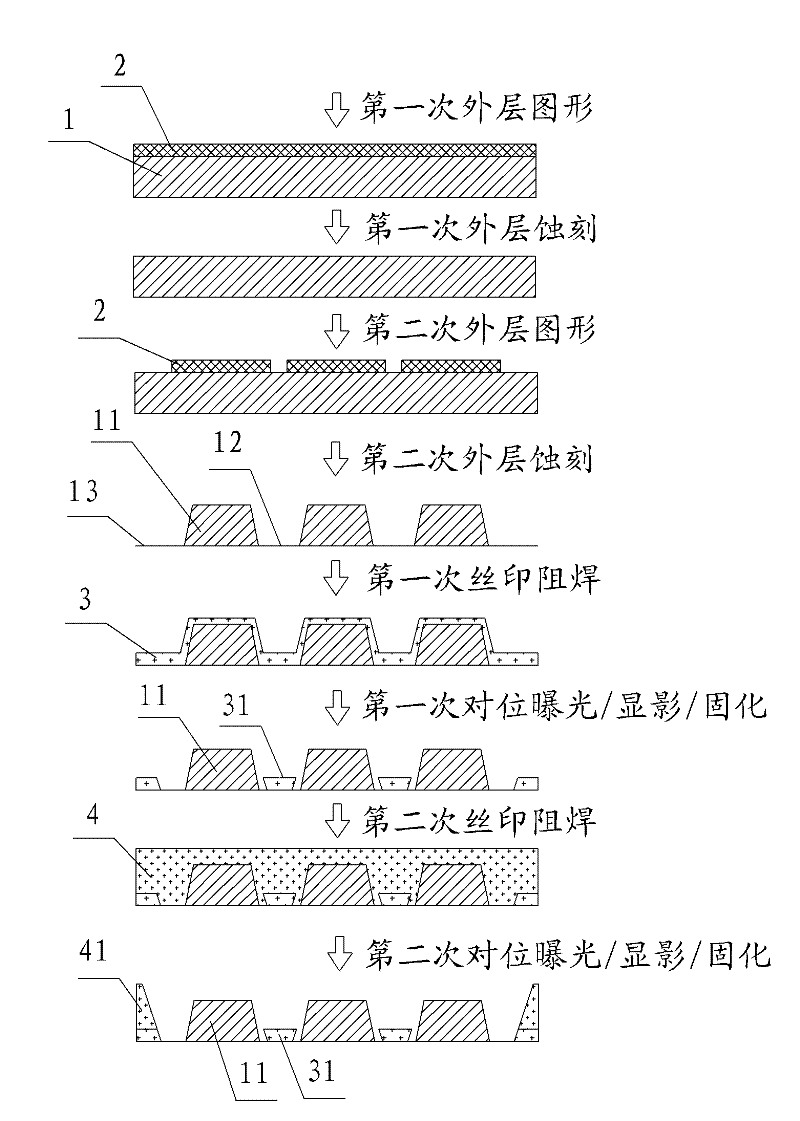
[0037] In order to describe the technical content, structural features, goals and effects of the present invention in detail, the following will be described in detail in combination with the accompanying drawings. Of course, the surface mount processing of thick copper circuit boards is not limited to the circuit boards of the above specifications, and it can also be applied to the surface mount processing of thick copper circuit boards such as 3OZ, 4OZ, and 6OZ.
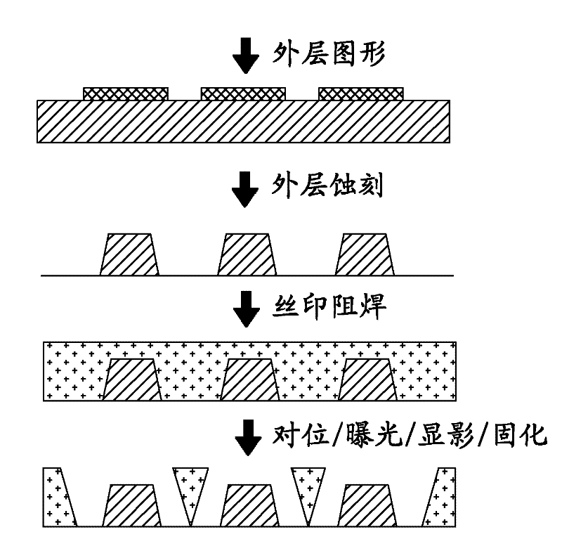
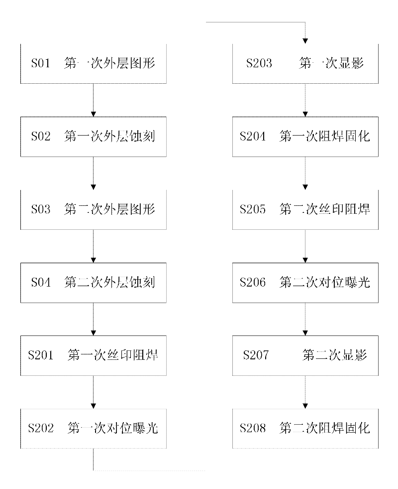
[0038] see figure 2 as well as image 3 , the present invention provides a kind of processing method of surface mount of thick copper circuit board, and the surface of thick copper circuit board comprises surface mount graphic area and circuit figure area, and the technological process of processing method is:
[0039] S01: The first outer layer pattern: Cover the circuit pattern area and the surface-mounted pattern area 1 with dry film 2, and expose the copper foil part that needs to be etched off in the line pa...
PUM
| Property | Measurement | Unit |
|---|---|---|
| Thickness | aaaaa | aaaaa |
Abstract
Description
Claims
Application Information