Method for analyzing chip failure

A failure analysis and chip technology, applied in electronic circuit testing, optical testing flaws/defects, non-contact circuit testing, etc., can solve problems such as difficult grinding and stripping accurate size parameters, save time and cost, and improve work efficiency Effect

Active Publication Date: 2011-11-23
SEMICON MFG INT (SHANGHAI) CORP +1
View PDF3 Cites 44 Cited by
  • Summary
  • Abstract
  • Description
  • Claims
  • Application Information

AI Technical Summary

Problems solved by technology

[0006] The technical problem to be solved by the present invention is to provide a chip failure analysis method to solve the problem that it is difficult to accurately

Method used


Image

  • Method for analyzing chip failure
  • Method for analyzing chip failure
  • Method for analyzing chip failure

Examples


Embodiment Construction

[0027] In order to make the above objects, features and advantages of the present invention more comprehensible, specific implementations of the present invention will be described in detail below in conjunction with the accompanying drawings.

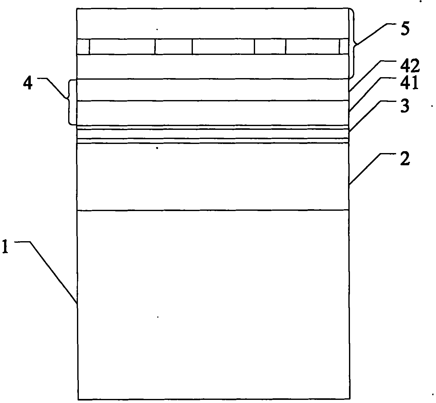
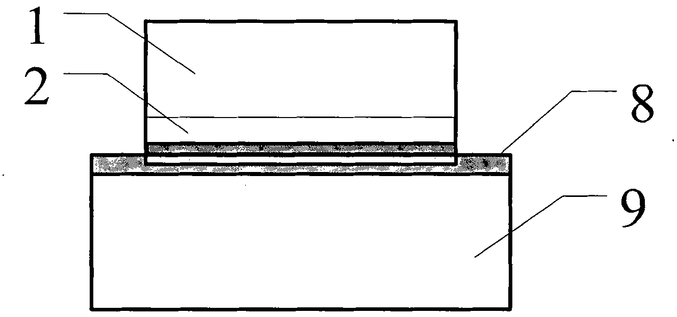
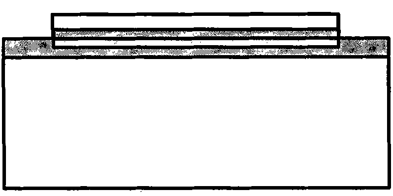
[0028] The chip failure analysis method described in the present invention can be widely used in the failure analysis of memory chips and other semiconductor chips, and can be realized in various alternative ways. The following is an illustration through a preferred embodiment, and of course the present invention is not limited In this specific embodiment, general substitutions known to those skilled in the art undoubtedly fall within the protection scope of the present invention.

[0029] Secondly, the present invention is described in detail using schematic diagrams. When describing the embodiments of the present invention in detail, for the convenience of illustration, the schematic diagrams are not partially enlarged according to th...


PUM


Abstract

The invention provides a method for analyzing chip failure, which is used for detecting defect characteristics of a chip grid and comprises the following steps: removing most of a substrate and an active region of a chip to be subjected to failure analysis through mechanical grinding; removing the remained substrate and active region of the chip through wet etching; removing most of a gate oxide layer of the chip through dry etching, wherein the remained gate oxide layer is used for protecting a first polysilicon layer of the grid; and detecting whether the defect characteristics exist on thefirst polysilicon layer or not. By utilizing the method provided by the invention, the chip can be accurately stripped to the bottom of the first polysilicon layer of the grid, the accurate size parameters of the bottom of the first polysilicon layer can be measured, the working efficiency can be greatly improved, and the time can be saved.

Description

technical field [0001] The invention relates to the field of semiconductor failure analysis, in particular to a chip failure analysis method. Background technique [0002] In the modern integrated circuit manufacturing process, chip processing needs to go through a series of chemical, optical, metallurgical, thermal processing and other process links. Each process may introduce various defects. At the same time, due to the continuous shrinking of feature size, the cost of various processing facilities has also risen sharply, so the loss caused by device defects is extremely expensive. Under such conditions, it becomes an indispensable link in the manufacture of integrated circuits to analyze the cause of failure and reduce device defects through verification testing. Through the failure analysis work, it can help IC designers find design defects and mismatch of process parameters, and also help IC application personnel find problems such as improper use of design or operat...

Claims


Application Information

Patent Timeline
IPC IPC(8): G01R31/28G01R31/311G01N21/88
Inventor 赖李龙高慧敏陈宏领
Owner SEMICON MFG INT (SHANGHAI) CORP
Why Eureka
Try Eureka