PN junction isolating structure and forming method thereof

A technology of isolation structure and PN junction, which is applied in the direction of electrical components, circuits, semiconductor devices, etc., can solve problems such as occupancy and large chip area, achieve simple process, reduce the possibility of self-doping, and better control the epitaxial growth process Effect

Inactive Publication Date: 2011-11-23
ADVANCED SEMICON MFG CO LTD
View PDF2 Cites 11 Cited by
  • Summary
  • Abstract
  • Description
  • Claims
  • Application Information

AI Technical Summary

Problems solved by technology

[0004] However, in order to enable the upper and lower isolation regions 105 and the lower isolation region 103 to be butted up and down after being diffused, long-term high-temperature annealing is required, and while the upper and lower isolation regions 105 and the lower isolation region 103 are diffused, severe lateral diffusion will also occur. causing it to occupy a large amount of chip area

Method used


Image

  • PN junction isolating structure and forming method thereof
  • PN junction isolating structure and forming method thereof
  • PN junction isolating structure and forming method thereof

Examples


Embodiment Construction

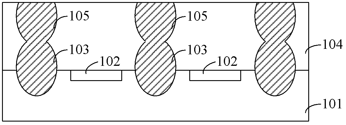
[0034] In the formation process of the PN junction isolation structure in the prior art, the lower isolation region and the upper isolation region are often formed first, and then the two are connected up and down through annealing advancement, but long-term annealing advancement will cause severe lateral diffusion, making The PN junction isolation structure occupies a larger chip area.

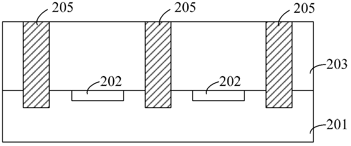
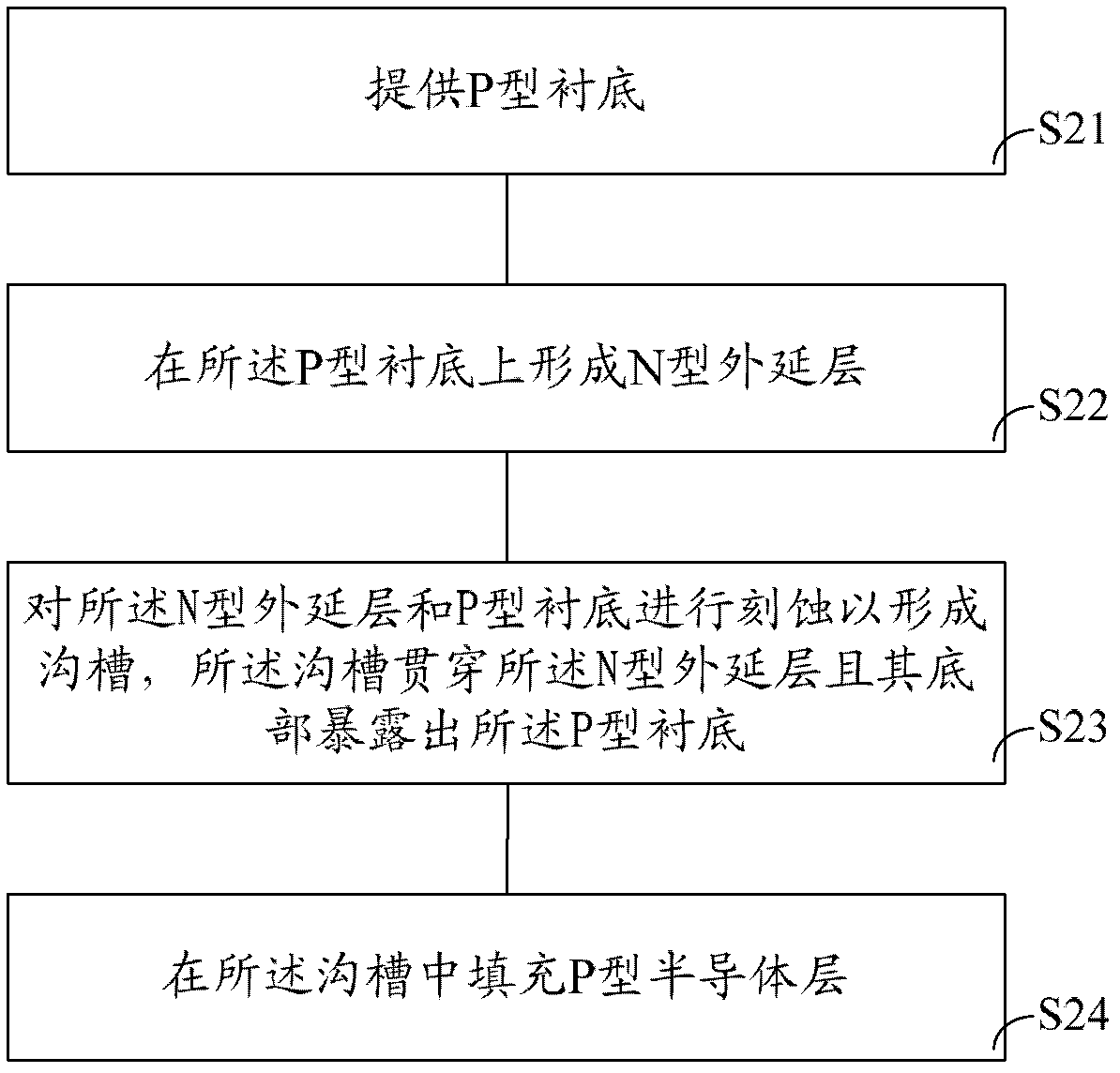
[0035] In the PN junction isolation structure and its forming method of the embodiment of the present invention, a trench is first formed on the N-type epitaxial layer, and then a P-type semiconductor layer is filled in the trench, which avoids the heat generated during the formation of the traditional PN junction isolation structure. The problem is that the process is long, the lateral diffusion is serious, and the isolation structure occupies a large chip area, and the doping concentration of the P-type semiconductor layer in the PN junction isolation structure of this embodiment is relative...


PUM


Abstract

The invention provides a PN junction isolating structure and a forming method thereof. The PN junction isolating structure comprises a P type substrate, an N type epitaxial layer, a groove and a P type semiconductor layer, wherein the N type epitaxial layer is positioned on the P type substrate; the groove passes through the N type epitaxial layer; the P type substrate is exposed out of the bottom of the groove; and the P type semiconductor layer is filled in the groove. The PN junction isolating structure contributes to reducing the occupied chip area, and has a simple process and high operability.

Description

technical field [0001] The invention relates to the technical field of semiconductor devices and semiconductor processes, in particular to a PN junction isolation structure and a forming method thereof. Background technique [0002] The PN junction isolation structure is an isolation structure widely used in semiconductor technology, and is mainly used in the manufacturing process of bipolar integrated circuits. figure 1 A PN junction isolation structure in the prior art is shown, mainly comprising: a P-type substrate 101; an antimony buried layer 102 formed on the P-type substrate 101; an N-type epitaxial layer 104; And the lower isolation region 103 in the N-type epitaxial layer 104; the upper isolation region 105 in the N-type epitaxial layer 104, the upper isolation region 105 and the lower isolation region 103 are connected up and down, and the doping type of both is P type. A PN junction is formed between the P-type doped upper isolation region 105 and the lower isola...

Claims


Application Information

Patent Timeline
Patent Type & Authority Applications(China)
IPC IPC(8): H01L29/06H01L21/761
Inventor 马清杰陈敏邵凯
Owner ADVANCED SEMICON MFG CO LTD
Why Eureka
Try Eureka