Light distribution structure of high-power LED (light-emitting diode)
A high-power, LED packaging technology, applied in electrical components, circuits, semiconductor devices, etc., can solve the problems of large interface loss of light on the LED light-emitting surface, and achieve the effect of reducing interface loss and increasing transmittance
- Summary
- Abstract
- Description
- Claims
- Application Information
AI Technical Summary
Problems solved by technology
Method used
Image
Examples
Embodiment Construction
[0020] In the following, the realization, functional features and advantages of the present invention will be further described in conjunction with the embodiments and accompanying drawings.
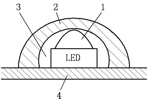
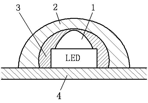
[0021] As we all know, when light exits or enters the interface, the closer the refractive index of the medium on both sides of the interface is, the smaller the interface loss will be. Therefore, filling the gap between the LED packaging lens and the light distribution lens with a transparent material having a refractive index similar to that of the above two lenses and eliminating the above air gap will greatly reduce the interface loss of light and increase the transmittance of light.
[0022] In a specific embodiment, in order to ensure that the air gap is completely eliminated without damaging the original shape and size parameters of the two lenses, a liquid filling material can be used, or a soft solid solidified from a liquid, such as silica gel, can be used.
[0023] Please refe...
PUM
 Abstract
Description
Claims
Application Information


