A ceramic substrate copper cladding and high-power electronic chip all-copper interconnect packaging scheme

A technology of ceramic substrates and electronic chips, applied in circuits, electrical components, electrical solid devices, etc., can solve the problems of reducing thermal and electrical conductivity of packaging, cost, and increasing the risk of packaging failure, so as to improve thermal and electrical conductivity, reduce interface loss, The effect of reducing the temperature of the copper clad process

Active Publication Date: 2022-07-15
SOUTH UNIVERSITY OF SCIENCE AND TECHNOLOGY OF CHINA
View PDF0 Cites 0 Cited by
  • Summary
  • Abstract
  • Description
  • Claims
  • Application Information

AI Technical Summary

Problems solved by technology

In order to ensure the combination of the chip mounting material and the substrate, usually the copper clad surface needs to be covered with silver, which is very expensive.
In addition, too many interfaces of different materials in the package will reduce the thermal and electrical conductivity of the package and increase the risk of package failure

Method used


Image

  • A ceramic substrate copper cladding and high-power electronic chip all-copper interconnect packaging scheme
  • A ceramic substrate copper cladding and high-power electronic chip all-copper interconnect packaging scheme
  • A ceramic substrate copper cladding and high-power electronic chip all-copper interconnect packaging scheme

Examples


Embodiment 1

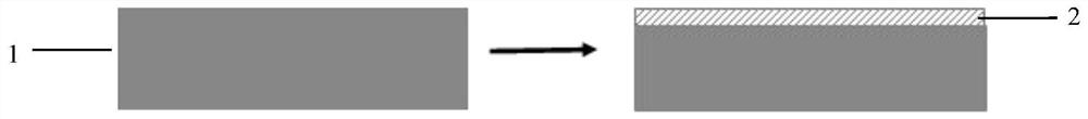
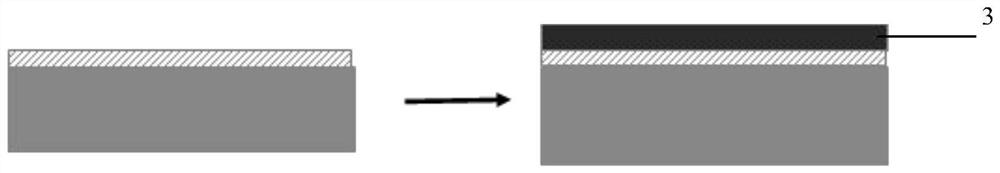
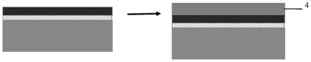
[0027] A preferred method for implementing a new design for copper cladding on a ceramic substrate and packaging, comprising the following preparation steps: vapor deposition of a 100nm Ti / 500nm copper layer on the surface of an alumina ceramic substrate; (2) coating the surface of the layer with a nano-copper cross-linking agent, according to the packaging The design needs to be printed into a circuit; (3) Then, place it in a nitrogen environment at a temperature of 100 ° C and bake for 30 minutes; (4) Place the chip on the baked substrate; (5) Coat the chip pad The nano copper paste is connected with the copper clip; (6) the whole chip is connected to the substrate through a hot pressing process, and a mixed gas of 8% hydrogen and 92% nitrogen is introduced, the pressure is raised to 15MPa, the sintering temperature is 300 ℃, and the sintering is 10min;

[0028] The above packaging results: the chip shearing force is 20MPa, and the thermal cycle test (-55℃~150℃) is more than ...

Embodiment 2

[0030] A preferred method for implementing a new design for copper cladding on a ceramic substrate and packaging, comprising the following preparation steps: vapor deposition of a 100nm Ti / 1000nm copper layer on the surface of an alumina ceramic substrate; (2) coating the surface of the layer with a nano-copper cross-linking agent, according to the packaging The design needs to be printed into a circuit; (3) Then, place it in a nitrogen environment at a temperature of 100 ° C and bake for 30 minutes; (4) Place the chip on the baked substrate; (5) Coat the chip pads with nanometers The copper paste is connected with the copper clip; (6) the whole chip is connected to the substrate through a hot pressing process, 8% hydrogen and 92% nitrogen are introduced, the pressure is raised to 15MPa, the sintering temperature is 300°C, and the sintering is 10min;

[0031] The above packaging results: the chip shearing force is 25MPa, and the thermal cycle test (-55℃~150℃) is more than 500 c...

Embodiment 3

[0033] A preferred method for implementing a new design for copper cladding and packaging on a ceramic substrate, comprising the following preparation steps: vapor deposition of a 500nm copper layer on the surface of an alumina ceramic substrate; (2) coating the surface of the layer with a nano-copper cross-linking agent, and printing according to packaging design requirements (3) Then, place the chip in a nitrogen environment, at a temperature of 100°C, and bake for 30 minutes; (4) Place the chip on the baked substrate; (5) Coat the chip pad with nano-copper paste and Copper clip connection; (6) The whole chip is connected to the substrate through a hot pressing process, 8% hydrogen and 92% nitrogen are introduced, the pressure is raised to 15MPa, the sintering temperature is 300°C, and the sintering is 10min;

[0034] The above package results: the chip shear force is 10MPa.


PUM


Abstract

The invention provides a copper-clad ceramic substrate and an all-copper interconnect packaging solution for high-power electronic chips. The specific steps include: S1 depositing a copper layer on the surface of the ceramic substrate as an adhesive layer; S2 coating the surface of the adhesive layer with nano-copper linking agent, printing a circuit including a ceramic substrate, an adhesive layer, and a nano-copper cross-linking agent, and baking to prepare a preform; S3, on the preform, install a copper-plated chip on the back; S4, on the metal welding of the chip The nano-copper cross-linking agent is placed on the plate to connect the copper clips; the S5 integrally sinters the preform, the chip, and the nano-copper cross-linking agent to connect the copper clips to complete the stable connection between the chip and the substrate. The new packaging design in this patent can solve the problem of ceramic coating. The difficulty of copper simplifies the manufacturing process of the substrate and the package, and greatly reduces the interface barrier in the package, improves the reliability of its work and meets the high current requirements of high-power electronic products.

Description

technical field [0001] The invention relates to the field of semiconductor packaging, in particular to a ceramic substrate copper cladding and an all-copper high-power electronic chip packaging and interconnection scheme. Background technique [0002] Ceramic substrates are widely favored in high-power electronic packaging due to their high thermal conductivity. In order to efficiently combine with chips and meet the requirements of high thermal conductivity and electrical conductivity, the surface of ceramic substrates needs to be covered with thick layers of metal such as copper foil or aluminum. A solid chip material is used to complete the connection with the chip, and conductive silver glue or sintered silver material is currently used as the intermediate chip loading material. In order to ensure the bonding between the mounting material and the substrate, the copper-clad surface usually needs to be coated with silver, which is very expensive. In addition, excessive pr...

Claims


Application Information

Patent Timeline
Patent Type & Authority Patents(China)
IPC IPC(8): H01L21/768H01L21/48H01L23/498H01L23/538
CPCH01L21/4853H01L21/76895H01L23/49811H01L23/49838H01L23/5386
Inventor 张卫红黄显机叶怀宇张国旗
Owner SOUTH UNIVERSITY OF SCIENCE AND TECHNOLOGY OF CHINA
Why Eureka
Try Eureka