A vertical cavity surface laser based on optical dielectric film passivation and its preparation method
A technology of optical media and vertical cavity surface, applied in lasers, laser components, semiconductor lasers, etc., can solve the problems of chip performance being deeply affected by the process, increasing the complexity of the process, and increasing the cost of chip manufacturing, so as to reduce production costs , Improve efficiency and increase cost rate
- Summary
- Abstract
- Description
- Claims
- Application Information
AI Technical Summary
Problems solved by technology
Method used
Image
Examples
Embodiment 1
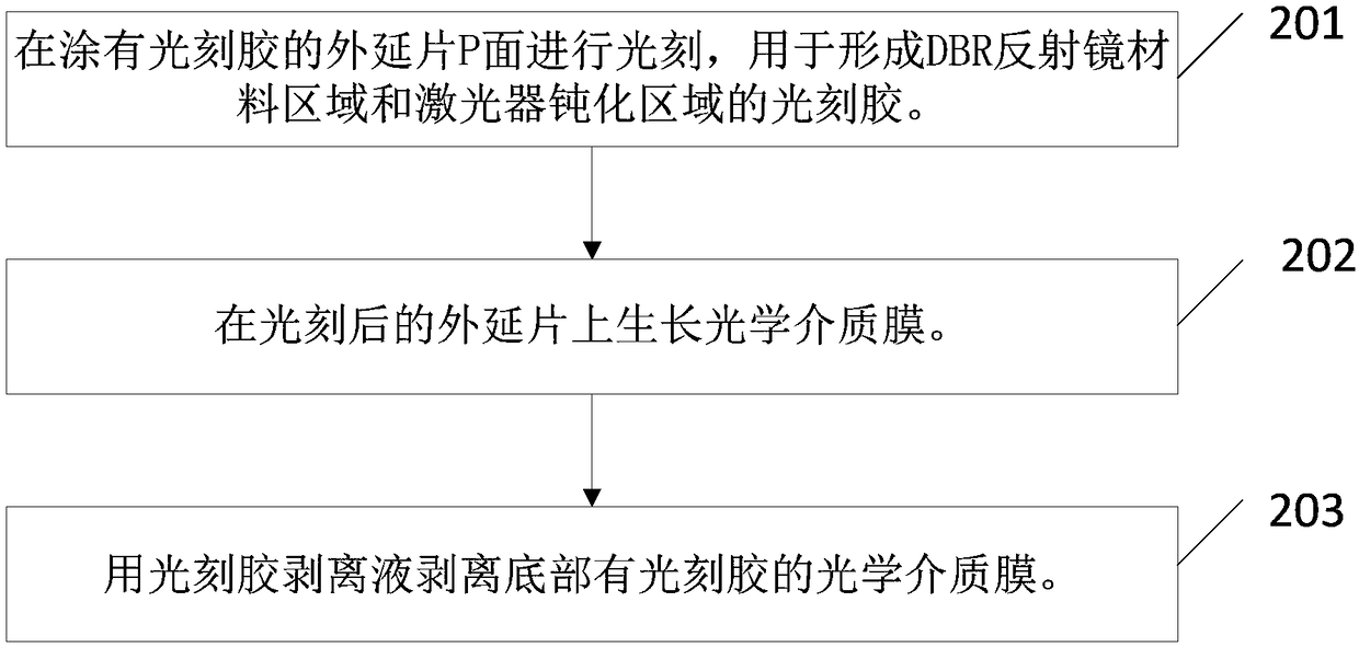
[0084] An embodiment of the present invention provides a method for fabricating a vertical cavity surface laser based on optical dielectric film passivation, such as figure 1 As shown, the preparation method specifically includes the following steps:
[0085] In step 201, photolithography is performed on the surface P of the epitaxial wafer coated with photoresist to etch the photoresist used to form the DBR mirror material region and the laser passivation region.
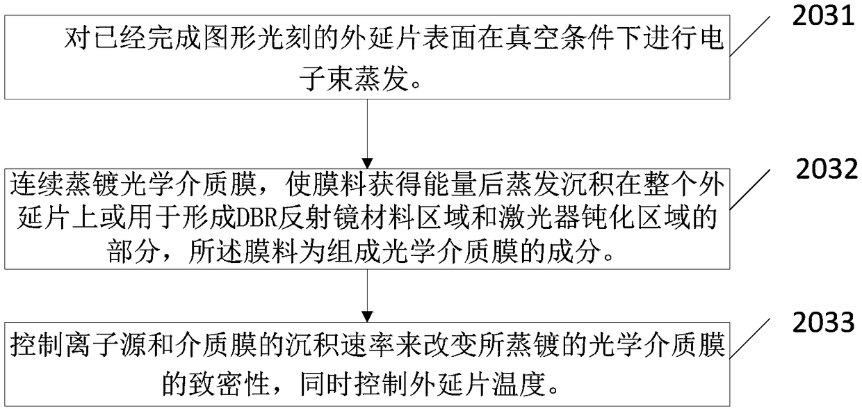
[0086] In step 202, an optical dielectric film is grown on the epitaxial wafer after photolithography.
[0087] In step 203, the optical medium film with the photoresist at the bottom is stripped with a photoresist stripper.
[0088] In the embodiment of the present invention, the preparation of the passivation film and the material of the DBR reflector is completed in the same vacuum chamber at one time, which not only improves the performance of the laser, but also reduces the possible damage caused by the numbe...
Embodiment 2
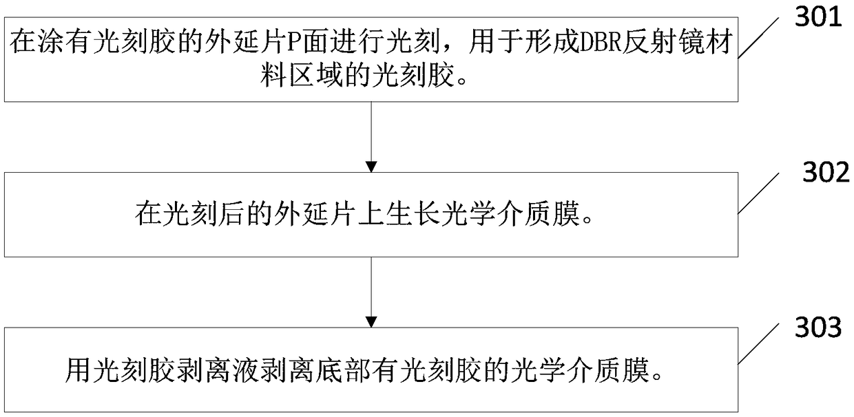
[0100] Corresponding to the preparation method of a vertical cavity surface laser based on optical dielectric film passivation described in Example 1, there is another embodiment in the present invention, a preparation of a vertical cavity surface laser based on an optical dielectric film as a DBR material method, using optical dielectric film as DBR reflector material, such as image 3 shown, including:
[0101] In step 301, photolithography is performed on the surface P of the epitaxial wafer coated with photoresist to form the photoresist in the material region of the DBR reflector.
[0102] In step 302, an optical dielectric film is grown on the epitaxial wafer after photolithography.
[0103] In step 303, the optical medium film with the photoresist at the bottom is stripped with a photoresist stripper.
[0104] The laser of the present invention adopts the optical dielectric film as the DBR mirror material, which reduces the series resistance, absorption loss and inter...
Embodiment 3
[0115] Corresponding to the preparation method of a vertical cavity surface laser based on the passivation of the optical dielectric film described in Example 1, there is also an embodiment in the present invention, wherein the laser uses the optical dielectric film as the passivation medium of the laser cavity surface film, such as Figure 5 Shown, described passivation dielectric film preparation process comprises:
[0116] In step 401, photolithography is performed on the surface P of the epitaxial wafer coated with photoresist, which is used for the photoresist in the passivation region of the laser cavity surface.
[0117] In step 402, an optical dielectric film is grown on the epitaxial wafer after photolithography.
[0118] In step 403, the optical medium film with the photoresist at the bottom is stripped with a photoresist stripper.
[0119] In a specific implementation, the step 402 can usually be implemented by the following steps, such as Image 6 Shown:
[012...
PUM
 Abstract
Description
Claims
Application Information


