Method for producing III-n layers, and III-n layers or III-n substrates, and devices based thereon
A III-N, substrate technology, applied in chemical instruments and methods, semiconductor/solid-state device manufacturing, crystal growth, etc., can solve problems such as not suitable for III-N wafers
- Summary
- Abstract
- Description
- Claims
- Application Information
AI Technical Summary
Problems solved by technology
Method used
Image

Examples
Embodiment 1
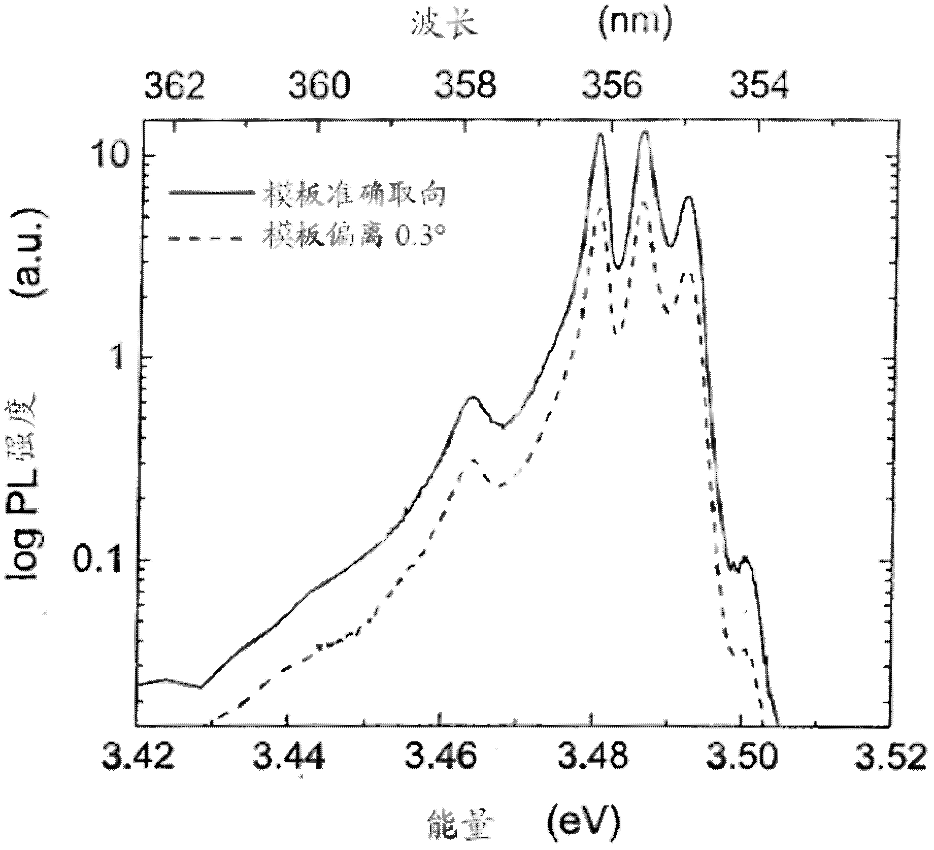
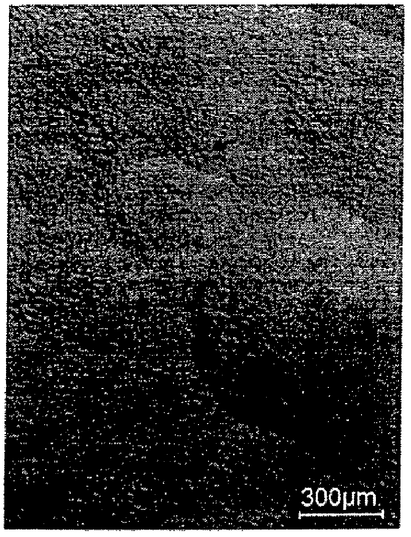
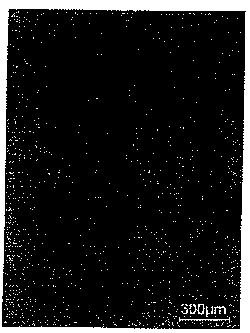
[0048] As an example, in an Aixtron 200 / 4RF-S MOVPE system, thin GaN layers can be grown on a sapphire heterogeneous substrate with a 0.3° misorientation. For example, the thickness of the thin GaN layer is less than 2 microns, in particular between 1 micron and 2 microns. Templates were unloaded from the MOVPE reactor and loaded onto an Aixtron LP-HVPE reactor. There, a thick GaN layer of a few hundred micrometers is grown on the template. For example, the operating conditions for HVPE treatment are: temperature between 1040°C and 1075°C, pressure between 900 mbar and 1000 mbar, N / III ratio of about 40, carrier gas of about 50% hydrogen and about 50% Nitrogen gas mixture. The growth rate in this example was about 40 microns / hour. By using a heterogeneous substrate with micro-orientation differences, the surface morphology was significantly improved after HVPE growth. Even with thick GaN layers of 40 microns or thicker, the surface morphology can be compared to much thinne...
Embodiment 2
[0050] The general framework of the present invention is that several templates on a sapphire heterogeneous substrate with misorientation and a conventional template on a sapphire heterogeneous substrate with accurate orientation are performed by using side by side in the same HVPE process. Compared.
[0051] All HVPE growth processing is done in an AIXTRON single wafer HVPE system with a horizontal quartz reactor. Metal Ga is delivered to the substrate by HCI gas in the usual manner. Ammonia was used as nitrogen source. The Ga source was operated at 850°C, while the substrate region was heated to 1040-1075°C. A 1:1 mixture of nitrogen and hydrogen was used as the carrier gas. The experiments were carried out at atmospheric pressure and a N / III ratio of approximately 40.
[0052] All HVPE growth layers were deposited on a GaN template grown by MOVPE on a two-inch thick sapphire wafer as the foreign substrate. Parallel use of four different templates is possible by loading...
Embodiment 3
[0059] The processing procedure described in Embodiment 2 is modified as follows:
PUM
| Property | Measurement | Unit |
|---|---|---|
| mean roughness | aaaaa | aaaaa |
| surface roughness | aaaaa | aaaaa |
| surface roughness | aaaaa | aaaaa |
Abstract
Description
Claims
Application Information
 - R&D
- Intellectual Property
- Life Sciences
- Materials
- Tech Scout
- Unparalleled Data Quality
- Higher Quality Content
- 60% Fewer Hallucinations
Browse by: Latest US Patents, China's latest patents, Technical Efficacy Thesaurus, Application Domain, Technology Topic, Popular Technical Reports.
© 2025 PatSnap. All rights reserved.Legal|Privacy policy|Modern Slavery Act Transparency Statement|Sitemap|About US| Contact US: help@patsnap.com