Back-illuminated sensor process

A back-illuminated, sensor element technology, applied in the direction of electric solid-state devices, semiconductor devices, electrical components, etc., can solve problems such as device degradation, influence on leakage current or dark current, negative impact on performance, etc., and achieve the effect of reducing changes

Inactive Publication Date: 2011-12-14
TAIWAN SEMICON MFG CO LTD
View PDF5 Cites 10 Cited by
  • Summary
  • Abstract
  • Description
  • Claims
  • Application Information

AI Technical Summary

Problems solved by technology

However, it is well known that stress on the substrate or sensing layer during BSI sensor processing can affect the leakage current or dark current
In particular, stress on the device substrate or sensing layer can be caused by subsequent color filter processing and / or device packaging after leaving the manufacturing facility, which can cause changes in dark current and the resulting negative impact on device performance or may even cause device degradation
[0005] Thus, while existing methods of fabricating semiconductor devices have been generally adequate for their intended purposes, they have not been satisfactory in every respect

Method used


Image

  • Back-illuminated sensor process
  • Back-illuminated sensor process
  • Back-illuminated sensor process

Examples


Embodiment Construction

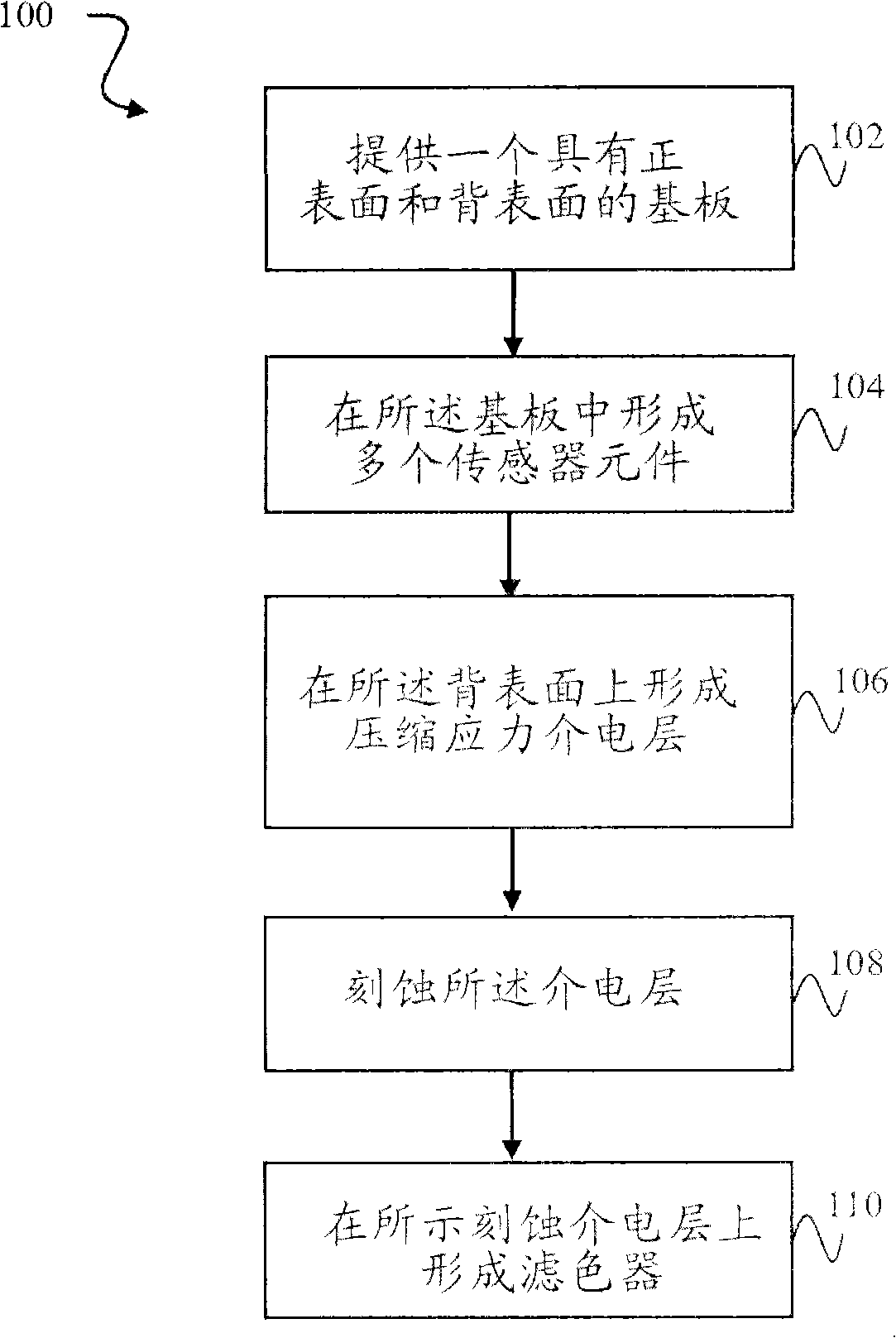
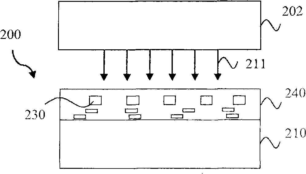
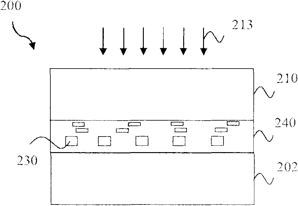
[0035] The present invention relates generally to the fabrication of semiconductor devices, and more particularly to methods of providing sensor isolation features of semiconductor substrates and devices fabricated using these methods.

[0036] It is understood that the following provides many different embodiments or examples for implementing different components of various embodiments. Specific examples of components and arrangements are described below to simplify the present invention. Of course, these are merely examples and are not intended to be limiting. For example, references below to a first component being formed "over" or "on" a second component may include embodiments in which the first and second components are formed in direct contact, and may also include references to the first and second components. Embodiments where additional components are formed between components such that the first and second components may not be in direct contact. In addition, the ...


PUM


Abstract

The present disclosure provides methods and apparatus for reducing dark current in a backside illuminated semiconductor device. In one embodiment, a method of fabricating a semiconductor device includes providing a substrate having a frontside surface and a backside surface, and forming a plurality of sensor elements in the substrate, each of the plurality of sensor elements configured to receive light directed towards the backside surface. The method further includes forming a dielectric layer on the backside surface of the substrate, wherein the dielectric layer has a compressive stress to induce a tensile stress in the substrate. A backside illuminated semiconductor device fabricated by such a method is also disclosed.

Description

[0001] priority date [0002] This application claims priority to US Provisional Application Serial No. 61 / 353,951 (Attorney No. 24061.1524), filed June 11, 2010, the entire contents of which are incorporated herein by reference. technical field [0003] The invention relates to a back-illuminated sensor technology. Background technique [0004] In semiconductor technology, backside illuminated (BSI) sensors are used to sense a certain amount of exposure light that hits the back surface of a substrate or sensing layer. A backside illuminated sensor can be formed on a substrate, and light irradiated onto the back surface of the substrate can reach the sensor. However, it is well known that the stress on the substrate or sensing layer will affect the leakage current or dark current during the processing of BSI sensors. In particular, stress on the device substrate or sensing layer can be caused by subsequent color filter processing and / or device packaging after leaving the m...

Claims


Application Information

Patent Timeline
Patent Type & Authority Applications(China)
IPC IPC(8): H01L27/146
CPCH01L27/14621H01L27/14609H01L27/1463H01L27/14643H01L27/14627H01L27/1464
Inventor 杜友伦蔡嘉雄王俊智林稔杰伍寿国
Owner TAIWAN SEMICON MFG CO LTD
Why Eureka
Try Eureka