
A method of manufacturing touch screen bonding parts

A manufacturing process and a technology for laminating parts, which is applied in the field of improvement of touch screen anti-drop performance, can solve problems such as touch screen failure, electric field cannot be formed, and glass hardening cannot be achieved, so as to improve processing pass rate, improve drop resistance performance, and overall The effect of cost reduction

Inactive Publication Date: 2011-12-28
NANJING WALLY ELECTRONICS TECH
View PDF5 Cites 7 Cited by
  • Summary
  • Abstract
  • Description
  • Claims
  • Application Information

AI Technical Summary

Problems solved by technology

Once the ITO conductive glass used as the lower electrode is damaged, the ITO layer on the electroplated glass surface will also be damaged, and a uniform electric field cannot be formed, which directly leads to the failure of the touch screen and cannot be repaired.
[0004] 2. Chemically strengthens the glass, which may lead to failure of the hardened layer
In order to solve the problem that the touch screen is easy to break, touch screen manufacturers have proposed many solutions, including chemical strengthening on the original glass. The principle is to exchange with potassium ions in the glass by soaking in the solution to form a layer The dense potassium ion layer is used to improve the surface strength of the glass, but in the process of making the touch screen, it is inevitable to cut the glass, so that the dense hardened layer is destroyed, and the effect of glass hardening cannot be achieved at all. Even due to the high hardness of the strengthened glass, if there are cracks in the glass during the cutting process, its strength is not as good as that of glass that has not been chemically strengthened.
[0005] 3. Using physically strengthened glass, the cost is high and the thickness is large
Although this kind of glass has high strength, it is expensive to manufacture, and the thickness must be more than 3mm, which is not suitable for the characteristics of small, light and thin electronic products.

Method used


Image

  • A method of manufacturing touch screen bonding parts
  • A method of manufacturing touch screen bonding parts
  • A method of manufacturing touch screen bonding parts

Examples


Embodiment Construction

[0032] In order to make the content of the present invention more obvious and understandable, further description will be made below in conjunction with the accompanying drawings and specific embodiments.

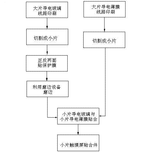
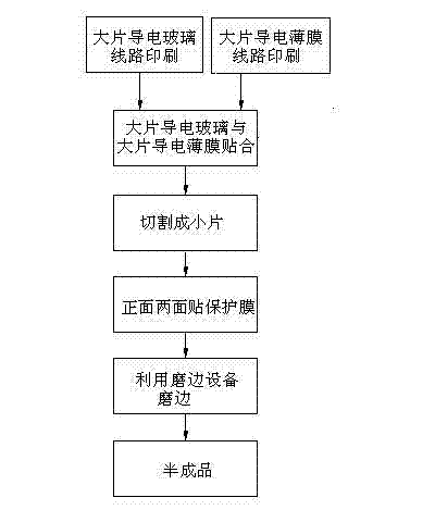
[0033] combine figure 1 , the manufacturing process method of the touch screen bonding part of the present invention, comprises the following steps:

[0034] (1). Print multiple corresponding functional circuit diagrams on large pieces of conductive glass and conductive film;

[0035] (2). Cut the large piece of conductive glass and conductive film that has been printed with the corresponding functional circuit diagram into small pieces of conductive glass and small pieces of conductive film suitable for a single touch screen;

[0036] (3). Use edging equipment to grind the cut small piece of conductive glass, so that the cut surface of each edge of the conductive glass is ground into a frosted curved surface;

[0037] (4). Bond the small piece of conductive glass and the...


PUM


Abstract

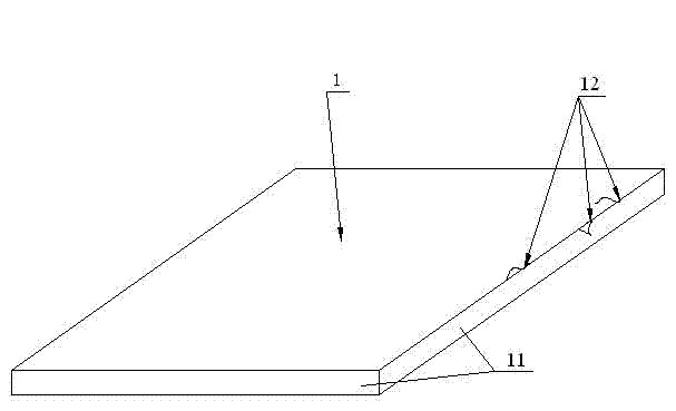
The invention relates to a manufacturing process of a touch screen bonding part. The bonding part is formed by bonding conductive glass and a conductive film. A touch screen uses a small bonding part, and a large bonding part contains a plurality of uncut small bonding parts. Fittings; in the process of making the fittings, the edging equipment is used to grind the cutting surface of each edge of the conductive glass in the small fittings into a frosted curved surface. The touch screen laminating part produced by the invention avoids the problems of stress concentration points and poor drop resistance in the cut surface of the ITO conductive glass substrate in conventional laminating parts. After the touch screen is made by using the invention, the stress when the touch screen falls can be effectively dispersed, and the qualified rate of products in the production of the touch screen can be improved. At the same time, because no strengthened glass substrate is used, the production cost is greatly reduced.

Description

technical field [0001] The invention relates to the technical field of improving the anti-drop performance of a touch screen, especially for a touch screen using indium tin oxide (ITO) conductive glass as a substrate. Background technique [0002] With the increasingly mature and saturated touch screen market, ordinary resistive touch screens are still favored by manufacturers of mobile phones and white goods due to their low price and relatively simple entry threshold. However, traditional film + glass structure touch screens are still It has limitations such as: [0003] 1. Easily broken by dropping or crushing. During the user's use, the mobile phone or other electronic equipment equipped with the touch screen accidentally falls to the ground, or when some squeezing actions, it is easy to cause damage to the touch screen, resulting in failure of the touch screen and making it unusable. The touch screen uses ITO conductive glass as the lower electrode, that is, a layer ...

Claims


Application Information

Patent Timeline
IPC IPC(8): G06F3/041
Inventor 缪健王春锋
Owner NANJING WALLY ELECTRONICS TECH
Learn More