Forming method of semiconductor structure and semiconductor structure

A technology of semiconductor and conductive structure, applied in the direction of semiconductor devices, semiconductor/solid-state device manufacturing, semiconductor/solid-state device components, etc., can solve problems such as the influence of semiconductor electrical performance

Active Publication Date: 2014-11-05
SHANGHAI HUAHONG GRACE SEMICON MFG CORP
View PDF5 Cites 0 Cited by
  • Summary
  • Abstract
  • Description
  • Claims
  • Application Information

AI Technical Summary

Problems solved by technology

Some interconnection layers or interconnection structures must remain insulating, while some interconnection structures or interconnection layers must remain conductive. If the control is not reasonable in the manufacturing process, resulting in the formation of interconnection structures or interconnection layers that need to be insulated. The electrical connection has a great impact on the electrical properties of the entire semiconductor

Method used


Image

  • Forming method of semiconductor structure and semiconductor structure
  • Forming method of semiconductor structure and semiconductor structure
  • Forming method of semiconductor structure and semiconductor structure

Examples


no. 1 example

[0049] Figure 4 to Figure 8 It is a structural cross-sectional schematic diagram of a method for forming a semiconductor structure according to the first embodiment of the present invention.

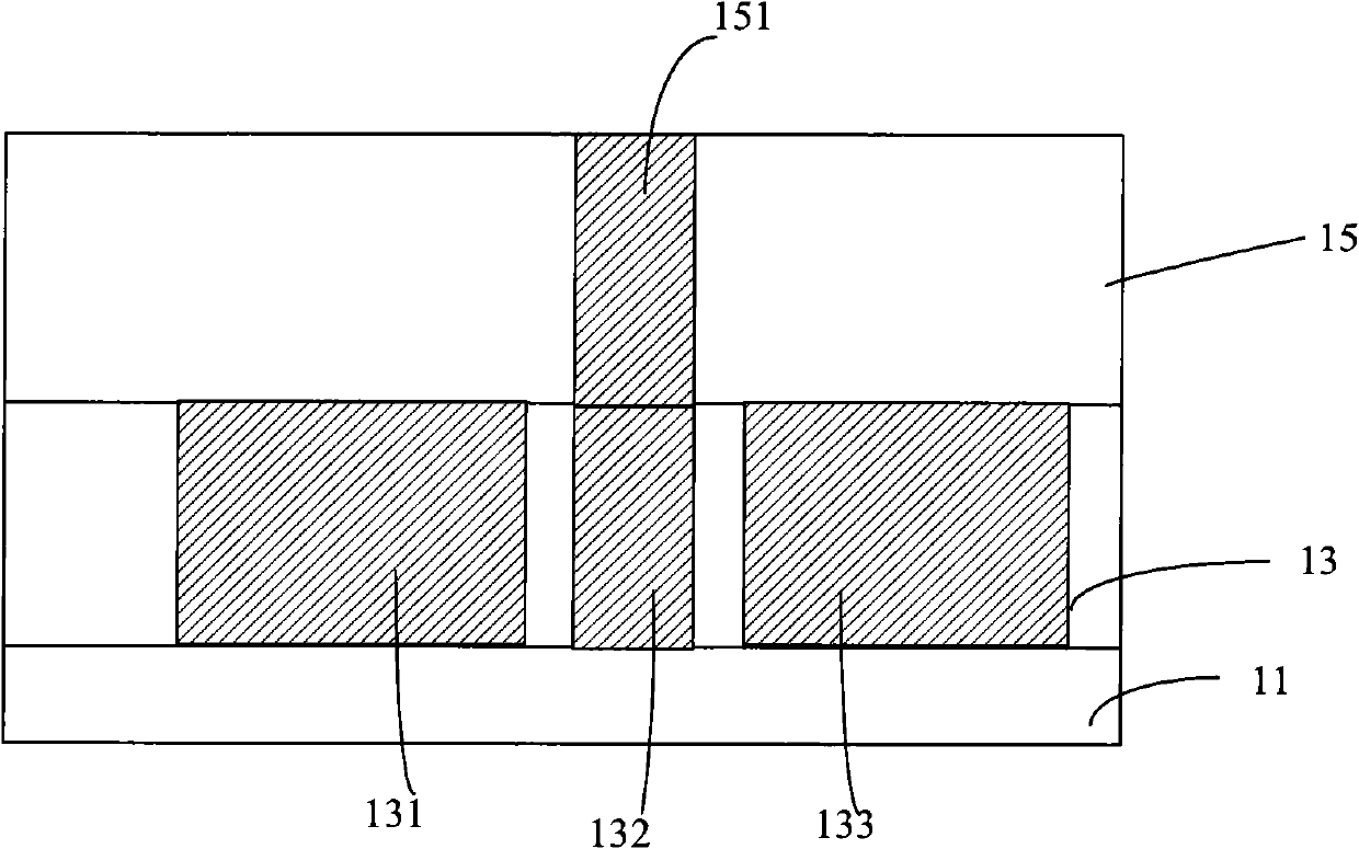
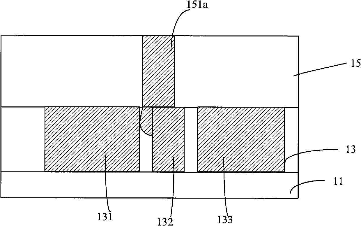
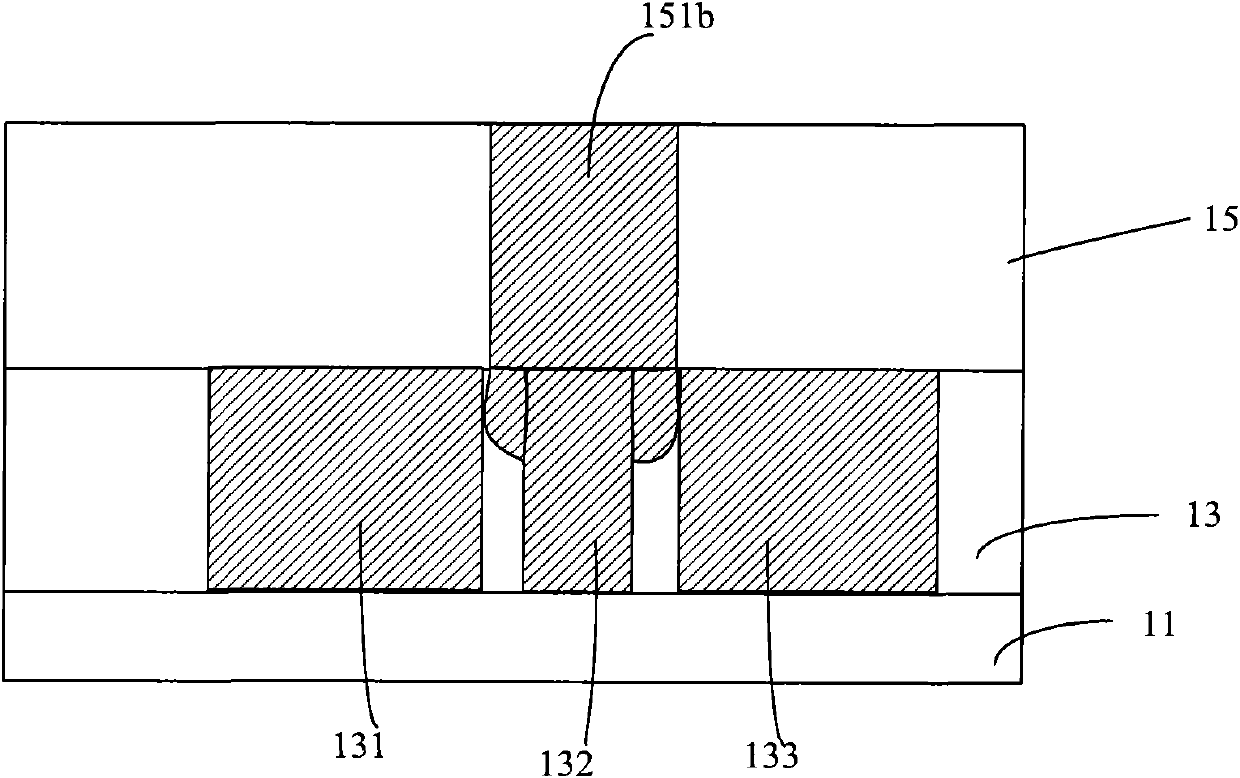
[0050] First, if Figure 4 As shown, a substrate 21 is provided, and a first dielectric layer 23 is formed on the substrate 21 . The base 21 is formed with conductive structures (not shown).

[0051] The first dielectric layer 23 can be fluorine-doped silicon oxide, carbon-doped silicon oxide, or a porous medium layer formed by liquid colloidal silicon oxide-based materials. In this embodiment, the first dielectric layer 23 is Fluorine-doped silicon oxide is formed by chemical vapor deposition or plasma enhanced chemical vapor deposition.

[0052] Such as Figure 5 As shown, a first interconnection layer 231 , a second interconnection layer 232 , and a third interconnection layer 233 are formed in the first dielectric layer 23 through its thickness. The specific formation process i...

no. 2 example

[0068] Figure 9 to Figure 12 It is a schematic cross-sectional view of a method for forming a semiconductor structure according to a second embodiment of the present invention.

[0069] First, if Figure 9 A substrate 31 is shown having conductive structures formed therein.

[0070] A first dielectric layer 33 and an etch stop layer 35 are formed on the substrate 31 .

[0071] The first dielectric layer 33 can be fluorine-doped silicon oxide, carbon-doped silicon oxide, or a porous medium layer formed by liquid colloidal silicon oxide-based materials. In this embodiment, the first dielectric layer 33 is Fluorine-doped silicon oxide is formed by chemical vapor deposition.

[0072] The etch barrier layer 35 can be silicon nitride or silicon oxynitride, and the thickness range of the etch barrier layer 35 is The etching barrier layer 35 is formed by chemical vapor deposition or plasma enhanced chemical vapor deposition. As an embodiment, the etch stop layer 35 is silicon ni...


PUM


Abstract

The invention provides a forming method of a semiconductor structure. The method comprises the following steps: providing a substrate with a conductive structure, wherein a first dielectric layer covering the conductive structure is formed on the substrate, the interior of the first dielectric layer is provided with a first interconnection layer which penetrates through the thickness of the first dielectric layer, the first interconnection layer is electrically connected with the conductive structure; forming an etch barrier layer on the first dielectric layer and the first interconnection layer; forming a second dielectric layer on the etch barrier layer; etching the second dielectric layer and the etch barrier layer until the first interconnection layer and a part of the first dielectric layer are exposed so as to form an opening; completely filling the opening with an interconnection structure, wherein the interconnection structure is electrically connected with the first interconnection layer. The invention also provides a semiconductor structure. According to the invention, the etch barrier layer is formed between the first dielectric layer and the second dielectric layer and is used as an interface for the first dielectric layer and the second dielectric layer; when the interconnection structure is etched, the interface can be timely discriminated, thus the phenomenon of over-etching on the first dielectric layer can be avoided.

Description

technical field [0001] The invention relates to a semiconductor manufacturing process, in particular to a method for forming a semiconductor structure and the semiconductor structure. Background technique [0002] In the manufacturing process of a semiconductor device, in order to electrically interconnect the multilayer structure located on the active region, it is necessary to form multiple interconnection layers. The interconnection layer can be formed by metal filling to achieve various functions such as connecting circuits, matching circuits, and changing signal phases. [0003] Such as figure 1 The semiconductor structure shown is formed by the following steps: providing a substrate 11, a conductive structure (not shown) is formed in the substrate 11, forming a first dielectric layer 13 on the substrate 11, etching the first dielectric layer 13 and Metal filling is performed to form the first interconnection layer 131, the second interconnection layer 132, and the th...

Claims


Application Information

Patent Timeline
Patent Type & Authority Patents(China)
IPC IPC(8): H01L21/768H01L23/528
Inventor 肖海波
Owner SHANGHAI HUAHONG GRACE SEMICON MFG CORP
Why Eureka
Try Eureka