Semiconductor device and formation method thereof

A technology for semiconductors and devices, applied in the field of semiconductor devices and their formation, can solve the problems of easy blocking of device contact, easy residues on the surface of semiconductor devices, device yield, yield impact, etc., so as to reduce device manufacturing costs, reduce quantity, The effect of strong removal

Active Publication Date: 2016-06-22
SEMICON MFG INT (SHANGHAI) CORP
View PDF5 Cites 3 Cited by
  • Summary
  • Abstract
  • Description
  • Claims
  • Application Information

AI Technical Summary

Problems solved by technology

[0004] However, in the prior art, after the epitaxial growth of boron-doped silicon germanium, the surface of the semiconductor device is prone to residues, thereby forming defects
This kind of defect is easy to block the contact between devices in the subsequent process, so these defects have a great impact on device yield and yield

Method used


Image

  • Semiconductor device and formation method thereof
  • Semiconductor device and formation method thereof
  • Semiconductor device and formation method thereof

Examples


Embodiment Construction

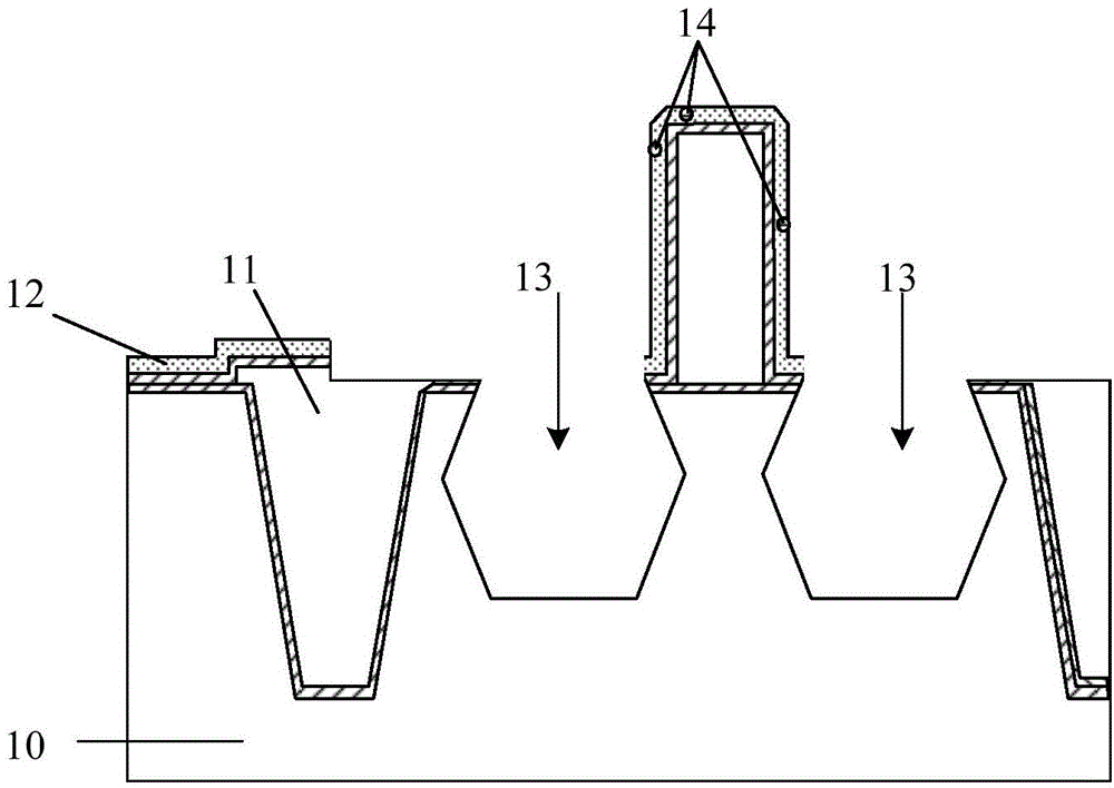
[0042] It can be seen from the background technology that in the prior art, the semiconductor device is cleaned after the epitaxial growth of the stress layer. The cleaning step is likely to form many tiny defects on the surface of the semiconductor device. The cause of the defect formation is analyzed in combination with the device formation process:

[0043] Such as figure 1 As shown, in the process of epitaxially growing boron-doped germanium silicon as a stress layer, after the isolation structure 11 is formed in the substrate 10, and before the epitaxial growth of the stress layer, the semiconductor device undergoes sequentially: depositing the protective layer 12 and etching the substrate to form Steps such as the groove 13, any one of these steps is likely to generate pollutants and etching residues (pollutants 14), and these pollutants remain on the surface of the protective layer 12 to form defects.

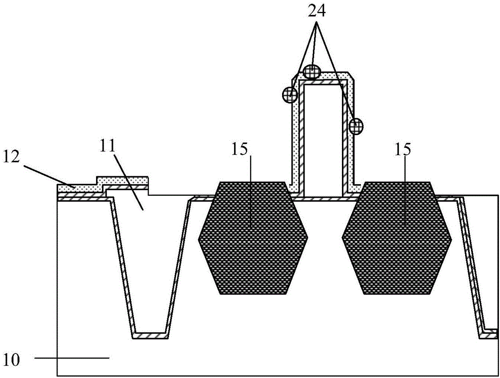
[0044] Such as figure 2 As shown, the pollutant 14 becomes the c...


PUM


Abstract

A semiconductor device and a forming method thereof, the forming method comprising: forming a base; forming a gate structure on the base; covering the base and the gate structure with a protective layer for protecting the gate structure; Forming grooves in the substrate on both sides of the pole structure; filling the grooves with semiconductor materials to form stress layers; performing ion doping on the semiconductor materials to form source regions and drain regions; after the step of covering the protective layer , before the step of filling the semiconductor material to form the stress layer, the method for forming the semiconductor device further includes: dry-cleaning the semiconductor device with a fluorine-containing gas. The invention can avoid a large number of defects generated after epitaxial growth, can effectively improve the yield rate in the device manufacturing process, and reduce the device manufacturing cost.

Description

technical field [0001] The invention relates to the field of semiconductor manufacturing, in particular to a semiconductor device and a forming method thereof. Background technique [0002] In the existing manufacturing process of semiconductor devices, the carrier mobility is usually improved by introducing stress into the channel region of the MOS device, thereby improving the performance of the MOS device. [0003] For PMOS devices, embedded silicon germanium technology is used to form source and drain regions to generate compressive stress in the channel region of the device, thereby improving carrier mobility. The so-called embedded silicon germanium technology refers to the formation of grooves in the regions where the source region and the drain region need to be formed on the semiconductor substrate, and then filling the grooves with silicon germanium material as a stress layer. Lattice mismatch creates compressive stress on the channel region. In a specific proces...

Claims


Application Information

Patent Timeline
Patent Type & Authority Applications(China)
IPC IPC(8): H01L29/78H01L29/10H01L21/336
Inventor 蔡国辉
Owner SEMICON MFG INT (SHANGHAI) CORP
Why Eureka
Try Eureka