Overlapped trench gate semiconductor component and manufacturing method thereof
A semiconductor and trench-type technology, applied in semiconductor/solid-state device manufacturing, semiconductor devices, semiconductor/solid-state device components, etc., can solve the problems of increasing cost and time-consuming, and achieve the goal of reducing Miller effect and feedback capacitance Effect
Inactive Publication Date: 2011-12-28
ANPEC ELECTRONICS CORPORATION
4 Cites 2 Cited by
AI-Extracted Technical Summary
Problems solved by technology
[0006] However, since the shielding electrode structure is located below the gate structure and in the same trench, multiple deposition and etch-back process ste...
Method used
...
Abstract
The invention provides an overlapped trench-type grid semiconductor component and a manufacturing method thereof. The overlapped trench-type grid semiconductor component comprises a semiconductor substrate, multiple shallow trenches arranged on the semiconductor substrate, a first conductive layer arranged in the shallow trenches, multiple deep trenches respectively arranged in the shallow trenches, a second conductive layer filled in the deep trenches, a source electrode metal layer and a grid electrode metal layer, wherein each deep trench extends to the semiconductor substrate below each shallow trench; the source electrode metal layer is electrically connected with the second conductive layer, and the grid electrode metal layer is electrically connected with the first conductive layer. Thus, the feedback capacitance between the first conductive layer and the semiconductor substrate can be reduced, the ratio of the input capacitance to the feedback capacitance can be increased, and the Miller effect can be further reduced.
Application Domain
TransistorSemiconductor/solid-state device details +2
Technology Topic
Feedback capacitanceCapacitance +6
Image
Examples
- Experimental program(1)
Example Embodiment
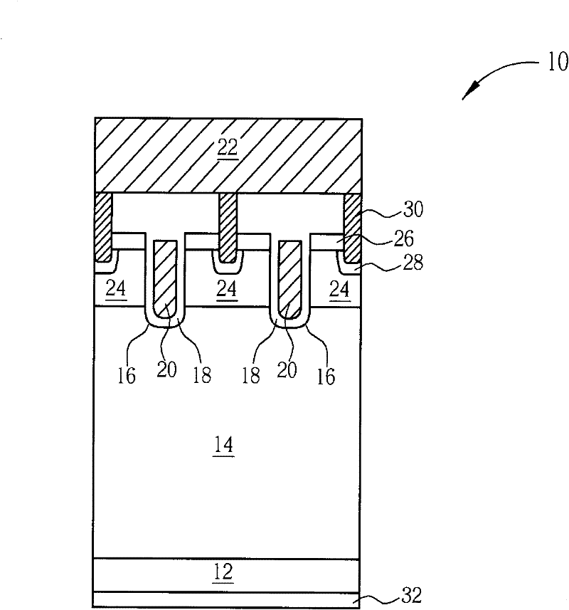
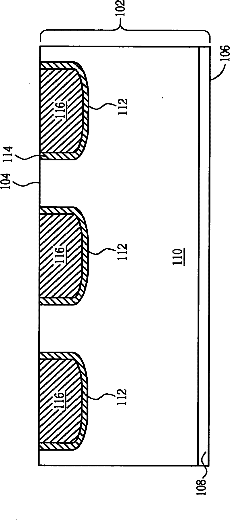
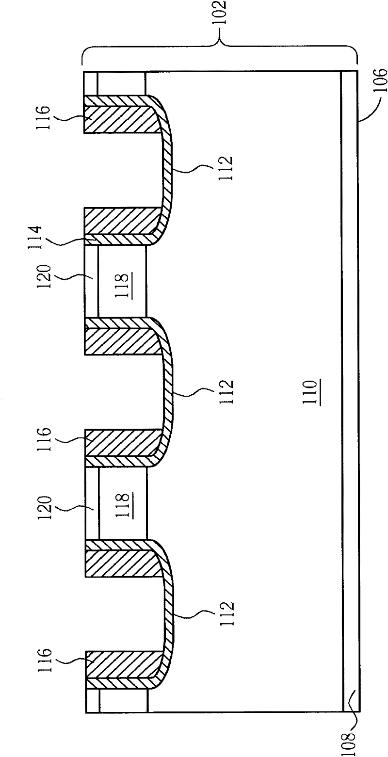
[0036] Please refer to Figure 2 to Figure 8 , Figure 2 to Figure 8 It is a schematic diagram of a method for manufacturing an overlapping trench gate semiconductor device according to a first embodiment of the present invention. Such as figure 2 As shown, first, a semiconductor substrate 102 is provided. The semiconductor substrate 102 has an upper surface 104 and an opposite lower surface 106. The semiconductor substrate 102 is composed of a substrate 108 and an epitaxial layer 110 formed on the substrate 108. constitute. The semiconductor substrate 102 has a first conductivity type, such as N-type or P-type. The semiconductor substrate 102 of the present embodiment takes the N-type as an example, and the invention is not limited thereto. The substrate 108 may be a silicon substrate, and both the substrate 108 and the epitaxial layer 110 have the first conductivity type. When the stacked trench gate semiconductor device is used as a power device, the epitaxial layer 110 is a lightly doped layer, and if a higher withstand voltage is desired, the thickness of the epitaxial layer 110 can be increased. In addition, the substrate 108 is a heavily doped layer, and the doping concentration of the substrate 108 is higher than the doping concentration of the epitaxial layer 110.
[0037] Then, a first mask pattern (not shown) is formed on the upper surface of the semiconductor substrate 102 by using the first photomask and the lithography process to define the position of each shallow trench, and an etching process is performed on the semiconductor substrate A plurality of shallow trenches 112 are formed on the upper surface 104 of 102, and then the first mask pattern is removed. Next, a chemical vapor deposition process is used to form a first insulating layer 114 on the upper surface 104 of the semiconductor substrate 102 and the surface of each shallow trench 112, and a planarization process is used to remove the first insulating layer 114 outside the shallow trench 112 An insulating layer 114. After that, a deposition process is used to form a first conductive layer 116 in the shallow trench 112 and fill each shallow trench 112, and then planarize to form a plurality of shallow trench structures. The first insulating layer 114 is used to electrically isolate the first conductive layer 116 from the semiconductor substrate 102, so that the first conductive layer 116 can be used as the gate of the overlapping trench gate semiconductor device. In addition, the first conductive layer 116 may be a doped semiconductor layer, such as a doped polysilicon layer, but is not limited thereto. Moreover, in this embodiment, the first insulating layer 114 and the first conductive layer 116 may be continuously formed, and then the planarization process may be performed.
[0038] Then like image 3 As shown, a second mask pattern (not shown), such as a photoresist pattern, is formed by using a second photomask in conjunction with a lithography process. Then, an ion implantation process with a second conductivity type is performed to implant ions of the second conductivity type into the semiconductor substrate 102 between any two adjacent shallow trenches 112. In this embodiment, the second conductivity type is P type, but it is not limited to this. The first conductivity type and the second conductivity type of the present invention can also be interchanged. Next, after removing the second mask pattern, a drive-in process is performed to diffuse the ions with the second conductivity type to a position approximately the same depth as the bottom of the shallow trench 112 to form a plurality of The base doped region 118 of the second conductivity type is between any two adjacent shallow trenches 112. Then, a third mask pattern (not shown) is formed by using a second photomask in conjunction with a lithography process, and then an ion implantation process with the first conductivity type is performed to implant the upper surface of the matrix doped region 118 Into the ions of the first conductivity type. After that, after removing the third mask pattern, a drive-in process is performed to diffuse the ions of the first conductivity type implanted in the base doped region 118 to respectively form a plurality of source doped regions 120 corresponding to the Above each matrix doped region 118. The doping concentration of the source doping region 120 is higher than the doping concentration of the epitaxial layer 110. In addition, the portion of each base doped region 118 adjacent to the first insulating layer 114 serves as the channel region of the overlapping trench gate semiconductor device, and each source doped region 118 serves as the source of the overlapping trench gate semiconductor device. pole. In addition, the second mask pattern and the third mask pattern of this embodiment may also be the same mask pattern, such as an oxide insulating layer.
[0039] Then, like Figure 4 As shown, a deposition process is performed to cover a third insulating layer 122 on the upper surface of the semiconductor substrate. Then, a fourth mask pattern (not shown) is formed using a third photomask in conjunction with a lithography process to define the positions of a plurality of deep trenches, and a part of the third insulating layer 122 and each shallow trench are respectively removed Part of the first conductive layer 116 in 112 is to expose part of the first insulating layer 114. The position of each deep trench is between the first conductive layer 116 in each shallow trench 112. In addition, the step of removing part of the first conductive layer 116 in each shallow trench 112 in the present invention is not limited to using the third mask pattern as a mask, and the third insulating layer 122 may also be used to define the position of the deep trench first. , And part of the first conductive layer 116 is exposed. Using the third insulating layer 122 as a mask, the exposed first conductive layers 116 are removed. In order to prevent the first conductive layer 116 directly under the third insulating layer 122 from being removed, the step of removing part of the first conductive layer 116 in this embodiment preferably uses an anisotropic etching process, such as a dry etching process.
[0040] After that, like Figure 5 As shown, a deposition process is performed to cover the upper surface 104 of the semiconductor substrate 102 with a nitride layer. The nitride layer may include an insulating material as an etch stop layer, such as silicon nitride, but is not limited thereto. Then, an etching process is performed to remove the nitride layer located above the third insulating layer 122 and at the bottom of the shallow trench 112, forming a protective spacer 124 only on the sidewall of the first conductive layer 116, and exposing each shallow Part of the first insulating layer 114 at the bottom of the trench 112. It is worth noting that the protective spacer 124 is used to protect the sidewalls of the first conductive layer 116 in each shallow trench 112 to prevent subsequent etching processes from eroding the first conductive layer 116 in each shallow trench 112 , Causing damage to the first conductive layer 116.
[0041] Then like Image 6 As shown, an etching process is performed to remove a portion of the exposed first insulating layer 114 and a portion of the semiconductor substrate 102 below it, so as to form a plurality of deep trenches 126. Each deep trench 126 is respectively disposed in each shallow trench 112, and each deep trench 126 penetrates the first conductive layer 116 and the first insulating layer 114 from the upper surface 104 of the semiconductor substrate 102, and extends to each shallow trench 112 below the semiconductor substrate 102. Then, a second insulating layer 128 is covered above the semiconductor substrate 102 and on the surface of each deep trench 126. Then, like Figure 7 As shown, a deposition process is performed to form a second conductive layer 130 on the second insulating layer 128, and fill each deep trench 126. Then, an etch-back process is performed to remove the second conductive layer 130 located outside each deep trench 126 so that the second conductive layer 130 fills each deep trench 126 to form a plurality of deep trench structures, which are filled in The second conductive layer 130 in each deep trench 126 is also located under each shallow trench 112. The second insulating layer 128 is used to electrically isolate the second conductive layer 130 from the first conductive layer 116 and the semiconductor substrate 102, and since the second insulating layer 128 also covers the first conductive layer 116, it can also be used for electrical Sexually isolates the first conductive layer 116 from the source metal layer subsequently fabricated thereon. In addition, the second conductive layer 130 may be a doped semiconductor layer, but is not limited thereto.
[0042] Then like Figure 8 As shown, a fifth mask pattern (not shown) is formed by using a fourth photomask in conjunction with a lithography process to define the positions of a plurality of source contact holes 132, and an etching process is performed on any two adjacent Each source contact hole 132 is formed between the shallow trenches 112, and each base doped region 118 is exposed, wherein each source contact hole 132 penetrates the second insulating layer 128, the third insulating layer 122 and each source doped District 120. Then, an ion implantation process of the second conductivity type is performed to form a source contact doped region 134 with the second conductivity type on the exposed surface of each base doped region 118, wherein each source contact doped The doping concentration of the region 134 is higher than the doping concentration of the base doping region 118, so as to reduce the resistance between the source doping region 120 and the first source contact plug 136. Then, a deposition process and an etch-back process are sequentially performed to form a first source contact plug 136 in each source contact hole 132, wherein each first source contact plug 136 is respectively disposed in each source The electrode doped region 120 penetrates the second insulating layer 128 and the third insulating layer 122, and each source contact doped region 134 is disposed between each first source contact plug 136 and each base doped region 118 . It should be noted that, in order to make the overlapping trench gate semiconductor device of the present invention have a smaller size, each of the first source contact plugs 136 is preferably formed by a tungsten process.
[0043] After that, a gate metal layer (not shown in Figure 8 ) And a source metal layer 138, and a drain metal layer 140 is formed on the bottom surface 106 of the semiconductor substrate 102. The source metal layer 138 directly covers the deep trench structure and the shallow trench structure, so that the second conductive layer 130 and each first source contact plug 136 of this embodiment can directly contact the source metal layer 138 and Electrically connected together. Moreover, each first source contact plug 136 can electrically connect each source doped region 120 and the source metal layer 138. So far, the overlapping trench gate semiconductor device 100 of the first embodiment has been completed.
[0044] Please refer to Picture 9 , Picture 9 It is a schematic top view of the stacked trench gate semiconductor device according to the first embodiment of the present invention. Such as Picture 9 As shown, the gate metal layer 142 is formed on one side of the source metal layer 138, is electrically isolated from the source metal layer, and overlaps a part of the first conductive layer 116. In addition, during the step of forming the first source contact plug 136, the method for fabricating an overlapping trench gate semiconductor device of this embodiment further includes forming a gate contact plug 144 on the first conductive layer 116 to make The gate contact plug 144 is disposed between the first conductive layer 116 and the gate metal layer 142 and electrically connects the first conductive layer 116 and the gate metal layer 142.
[0045] It is worth noting that during the operation of the conventional overlapping trench gate semiconductor device, the depletion region between the base doped region and the epitaxial layer is located in the epitaxial layer at approximately the same depth as the bottom of the shallow trench. However, in the overlapping trench gate semiconductor device fabricated in this embodiment, when the overlapping trench gate semiconductor device starts to operate, the first conductive layer gives the gate signal, and the second conductive layer gives the source The depletion region between the matrix doped region and the epitaxial layer extends down to the epitaxial layer at the same depth as the deep trench through the electric field generated by the second conductive layers on both sides. Thereby, the parasitic capacitance between the first conductive layer as the gate and the drain metal layer as the drain can be reduced due to the extension of the depletion region, thereby effectively reducing the feedback capacitance of the overlapping trench gate semiconductor device. In addition, with the control of the parasitic capacitance between the source and gate of the overlapping trench gate semiconductor device, the ratio of input capacitance (Ciss) to feedback capacitance (reverse transfer capacitance, Crss) (Ciss/ Crss), thereby reducing the impact of voltage surges caused by the Miller effect. Among them, the input capacitance is composed of the capacitance between the source and the gate and the capacitance between the drain and the gate.
[0046] In addition, the third insulating layer of this embodiment can be used to adjust the parasitic capacitance between the source metal layer and the first conductive layer, thereby controlling the capacitance between the source electrode and the gate electrode. The protective spacer of this embodiment is vertically arranged between the first conductive layer and the second conductive layer. Therefore, adjusting the thickness of the protective spacer can control the parasitic capacitance between the first conductive layer and the second conductive layer, thereby controlling the source. The size of the capacitance with the gate. Therefore, the overlapping trench gate semiconductor component of this embodiment can fix the capacitance between the source and the gate through the third insulating layer and the protective spacer, and then reduce the feedback capacitance to effectively increase the Ciss/Crss. For example, the Ciss/Crss of the known overlap trench gate semiconductor device is approximately 10, while the Ciss/Crss of the overlap trench gate semiconductor device manufactured by this embodiment can be increased to 30.
[0047] In addition, it is worth noting that, in order to effectively reduce the feedback capacitance and improve the Ciss/Crss, the known technique of forming a shielding electrode structure under the gate structure to improve the Ciss/Crss requires a lot of mask patterning processes to fabricate the gate. However, compared with the known overlapping trench gate semiconductor device, the present invention can achieve the same effect by forming a deep trench structure in a shallow trench structure, and only an additional mask pattern is needed. The overlapping trench-type gate semiconductor device of the present invention is manufactured, and therefore, the process and manufacturing cost can be effectively saved.
[0048] Please refer to Picture 10 , Picture 10 It is a schematic diagram of a method for manufacturing an overlapping trench-type gate semiconductor device according to a second embodiment of the present invention. In order to clearly compare the differences between the first embodiment and the second embodiment, the same components in the second embodiment and the first embodiment are marked with the same symbols, and the same steps will not be repeated. Such as Picture 10 As shown, compared with the first embodiment, the method of fabricating the overlapping trench gate semiconductor device 200 in this embodiment further includes the step of forming the deep trench and the step of forming the first source contact plug. The second insulating layer 128 and the second conductive layer 130 are covered with a fourth insulating layer 202, wherein the fourth insulating layer 202 is disposed between the second conductive layer 130 and the source metal layer 138. In addition, the first source contact plug 136 formed after the step of covering the fourth insulating layer 202 penetrates the fourth insulating layer 202.
[0049] Please refer to Picture 11 , Picture 11 It is a schematic top view of an overlapping trench gate semiconductor device according to the second embodiment of the present invention. Such as Picture 11 As shown, in the method of fabricating the overlapping trench gate semiconductor device 200 of this embodiment, in the step of forming the first source contact plugs 136, a plurality of second source contact plugs are also formed on the second conductive layer 130 204. The second source contact plug 204 penetrates the fourth insulating layer 202 to connect the source metal layer 138 and the second conductive layer 130.
[0050] To sum up, the overlapping trench gate semiconductor device of the present invention forms a deep trench in the shallow trench, so that the second conductive layer filled in the deep trench can generate an electric field to connect the matrix doped region and the epitaxial layer. The depletion region extends into the epitaxial layer at the same depth as the deep trench, thereby reducing the feedback capacitance between the first conductive layer as the gate and the drain metal layer, and the Ciss/Crss is increased, thereby improving the Miller effect.
[0051] The foregoing descriptions are only preferred embodiments of the present invention, and any equivalent changes and modifications made in accordance with the claims of the present invention should fall within the scope of the present invention.
PUM


Description & Claims & Application Information
We can also present the details of the Description, Claims and Application information to help users get a comprehensive understanding of the technical details of the patent, such as background art, summary of invention, brief description of drawings, description of embodiments, and other original content. On the other hand, users can also determine the specific scope of protection of the technology through the list of claims; as well as understand the changes in the life cycle of the technology with the presentation of the patent timeline. Login to view more.