Manufacturing method of vertical organic thin film transistor

A technology of organic thin film and production method, which is applied in the fields of semiconductor/solid-state device manufacturing, temperature recording method, electric solid-state device, etc. The effect of overcoming high costs

Inactive Publication Date: 2013-12-25
CPTF VISUAL DISPLAY (FUZHOU) LTD +1
View PDF5 Cites 0 Cited by
  • Summary
  • Abstract
  • Description
  • Claims
  • Application Information

AI Technical Summary

Problems solved by technology

[0008] In view of this, the object of the present invention is to provide a vertical organic thin film transistor, which can use a metal with good conductivity as the gate electrode, and an insulating layer with a predetermined thickness is arranged on it to solve the problem of withstand voltage and electrical characteristics. good question

Method used


Image

  • Manufacturing method of vertical organic thin film transistor
  • Manufacturing method of vertical organic thin film transistor
  • Manufacturing method of vertical organic thin film transistor

Examples


Embodiment Construction

[0036] The description of the present invention provides different examples to illustrate the technical features of different implementations of the present invention. Wherein, the configuration of each component in the embodiment is for clearly illustrating the content disclosed in the present invention, and is not intended to limit the present invention. In addition, part of the reference numerals in the figures in different embodiments is repeated for the purpose of simplifying the description, and does not imply the correlation between different embodiments.

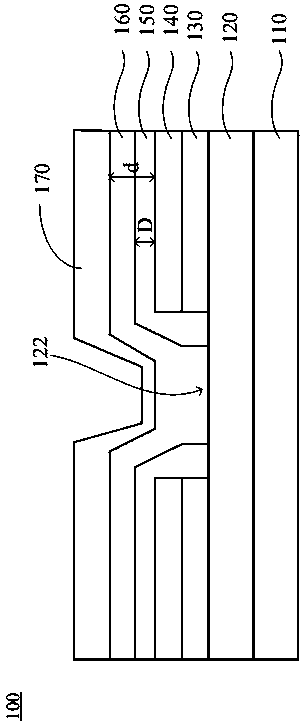
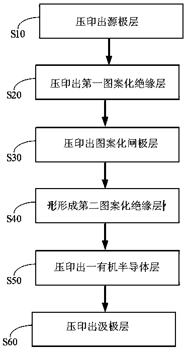
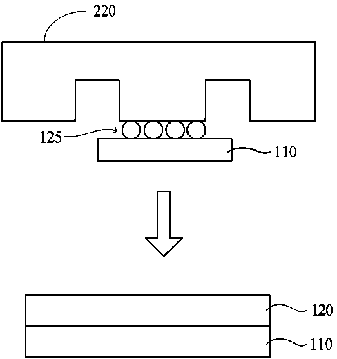
[0037] Please refer to figure 1 , figure 1 The vertical organic thin film transistor of the preferred embodiment of the present invention is shown, and it should be noted that it is not shown in actual scale. The vertical organic thin film transistor 100 includes a substrate 110, a source layer 120, a first patterned insulating layer 130, a patterned gate layer 140, a second patterned insulating layer 150, an organ...


PUM

PropertyMeasurementUnit
thicknessaaaaaaaaaa
thicknessaaaaaaaaaa

Abstract

The invention discloses a vertical organic thin film transistor and a manufacturing method thereof. The vertical organic thin film transistor comprises a source electrode layer, a first patterned insulation layer, a patterned gate electrode layer, a second patterned insulation layer, an organic semiconductor layer and a drain electrode layer, wherein the first patterned insulation layer is arranged on the source electrode layer, the patterned gate electrode layer is correspondingly arranged on the first patterned insulation layer, the second patterned insulation layer has the preset thickness and is covered on the patterned gate electrode layer, and the local surface of the source electrode layer is exposed out. The organic semiconductor layer is covered on the second patterned insulation layer and the local surface. The drain electrode layer is arranged on the organic semiconductor layer.

Description

technical field [0001] The present invention relates to a transistor and its manufacturing method, in particular to a vertical organic thin film transistor and its manufacturing method. Background technique [0002] The industry usually uses planar transistors as basic circuit components. Generally speaking, the so-called planar transistor means that the gate channel of the transistor is parallel to the surface of the substrate, and the drain / source regions of the transistor are respectively disposed at both ends of the gate channel. [0003] Planar transistors have the advantage of being easy to integrate with circuits, and thus are widely used in the manufacture of integrated circuits. However, planar transistors will occupy more surface area of ​​the substrate, so that the integration level of the integrated circuit cannot be increased. In addition, in the field of liquid crystal displays, as the picture becomes finer and finer, the area of ​​a single pixel becomes smal...

Claims


Application Information

Patent Timeline
Patent Type & Authority Patents(China)
IPC IPC(8): H01L51/05H01L51/30H01L51/40B41M5/26
Inventor 吴德峻翁守正李怀安
Owner CPTF VISUAL DISPLAY (FUZHOU) LTD
Why Eureka
Try Eureka