Terminal structure of MOSFET device and preparation method and application of terminal structure

A terminal structure and device technology, used in semiconductor/solid-state device manufacturing, semiconductor devices, electrical components, etc., can solve the problems of MOSFET device withstand voltage and leakage, and solve the problems of low withstand voltage and leakage, reduce costs, and suppress leakage. Effect

Pending Publication Date: 2020-09-29
SHENZHEN RUI ZHI CHEN TECH
View PDF0 Cites 0 Cited by
  • Summary
  • Abstract
  • Description
  • Claims
  • Application Information

AI Technical Summary

Problems solved by technology

[0004] The invention provides a terminal structure of a MOSFET device, which solves the problems of withstand voltage and leakage of the MOSFET device by setting a multi-layer closed silicon carbide groove ring outside the chip

Method used


Image

  • Terminal structure of MOSFET device and preparation method and application of terminal structure
  • Terminal structure of MOSFET device and preparation method and application of terminal structure
  • Terminal structure of MOSFET device and preparation method and application of terminal structure

Examples


Embodiment 1

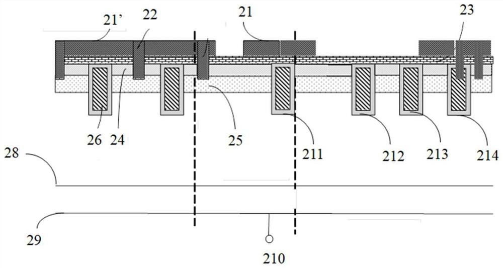
[0036] Such as figure 2 As shown, Embodiment 1 proposes a terminal structure of a MOSFET device, including more than one group of four silicon carbide trench rings (211, 212, 213, 214).

[0037] The silicon carbide trench rings (211, 212, 213, 214) are all closed rings.

[0038] The innermost silicon carbide trench ring (211) is connected to the low potential of the chip, and the innermost silicon carbide trench ring (211) is arranged on a side close to the gate metal (21).

[0039] The outermost groups of silicon carbide trench rings (214) are stop rings, the potential of the stop rings is connected to the scribing lane (23) of the chip, and the outermost silicon carbide trench rings (214) are set On the side close to the scribe lane (23).

[0040] Two sets of silicon carbide groove rings (212, 213) are further arranged between the innermost silicon carbide groove ring (211) and the outermost silicon carbide groove ring (214).

[0041] The preparation method of the termi...

Embodiment 2

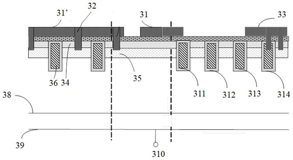
[0045] Such as image 3 As shown, Embodiment 2 proposes a terminal structure of a MOSFET device, including more than one group of four silicon carbide trench rings (311, 312, 313, 314).

[0046] The silicon carbide trench rings (311, 312, 313, 314) are all closed rings.

[0047] The innermost silicon carbide trench ring (311) is connected to the low potential of the chip.

[0048] The outermost groups of silicon carbide trench rings (314) are stop rings, the potential of the stop rings is connected to the scribing lane (33) of the chip, and the outermost silicon carbide trench rings (314) are set On the side close to the scribe lane (33).

[0049] Two sets of silicon carbide groove rings (312, 313) are further arranged between the innermost silicon carbide groove ring (311) and the outermost silicon carbide groove ring (314).

[0050] The preparation method of the terminal structure of the MOSFET device of embodiment 2, comprises the steps:

[0051] Connect the low potent...


PUM


Abstract

The invention relates to a terminal structure of an MOSFET device and a preparation method and application of the terminal structure. The terminal structure comprises more than one group of silicon carbide groove rings which are arranged on the periphery of an MOSFET device chip and are sequentially distributed from inside to outside, the silicon carbide groove rings are closed rings; the siliconcarbide groove ring on the innermost side is connected with the low potential of a chip; the silicon carbide groove ring on the outermost side is a cut-off ring, and the potential of the cut-off ringis connected with a scribing channel of the chip. According to the terminal structure of the MOSFET device, the silicon carbide groove is connected with the low potential of the chip at the inner side, so that the formation of a reverse channel is effectively inhibited, and electric leakage can be inhibited; the silicon carbide groove is connected with the high potential of the scribing channel onthe outer side, the isolation effect can be enhanced, and the closed annular design can prevent an electric leakage channel from being formed between the inner side and the outer side, so that the problems of voltage resistance and electric leakage of the MOSFET device are solved.

Description

technical field [0001] The invention belongs to the technical field of semiconductors, and in particular relates to a terminal structure of a MOSFET device and a preparation method and application thereof. Background technique [0002] Metal-Oxide-Semiconductor Field-Effect Transistor (MOSFET) is a field-effect transistor that can be widely used in analog circuits and digital circuits. The termination structure of MOSFETs usually uses silicon carbide trenches. Such as figure 1 As shown, the traditional manufacturing method of silicon carbide trench (SiC Trench MOS) includes the following steps: usually on a semiconductor substrate 9, a lightly doped N-type epitaxial layer 8 is formed, and a layer of carbon dioxide is grown on 8. Silicon layer, use the first P-well (P-well) photomask to define the P-type body region; then grow a thick silicon dioxide layer on the surface of the silicon carbide wafer, use the second trench (SiC Trench) photomask The mask defines the trench ...

Claims


Application Information

Patent Timeline
Patent Type & Authority Applications(China)
IPC IPC(8): H01L29/06H01L29/78H01L21/336
CPCH01L29/0623H01L29/0638H01L29/66068H01L29/7827
Inventor 裘三君
Owner SHENZHEN RUI ZHI CHEN TECH
Why Eureka
Try Eureka