Surface treatment device and method thereof

A surface treatment device and surface treatment technology, applied in the direction of electrical components, semiconductor/solid-state device manufacturing, circuits, etc., can solve problems affecting interface coverage and density, unfavorable component manufacturing process, etc.

Inactive Publication Date: 2012-01-11
IND TECH RES INST
View PDF5 Cites 0 Cited by
  • Summary
  • Abstract
  • Description
  • Claims
  • Application Information

AI Technical Summary

Problems solved by technology

[0003] For example, when a zinc oxide (ZnO) film is deposited in a low pressure chemical vapor deposition (LPCVD) manufacturing process, since the surface morphology of the zinc oxide film is often pyramid-shaped, a sharp film su

Method used


Image

  • Surface treatment device and method thereof
  • Surface treatment device and method thereof
  • Surface treatment device and method thereof

Examples


Embodiment Construction

[0070] In order to enable your review committee to have a further understanding and understanding of the characteristics, purpose and functions of the present invention, the relevant detailed structure and design concept of the device of the present invention will be explained below, so that the review committee can understand the present invention The characteristics are described in detail as follows:

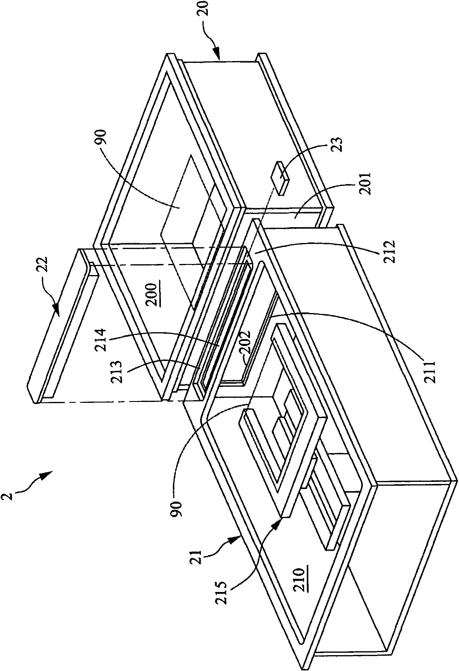
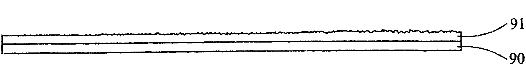
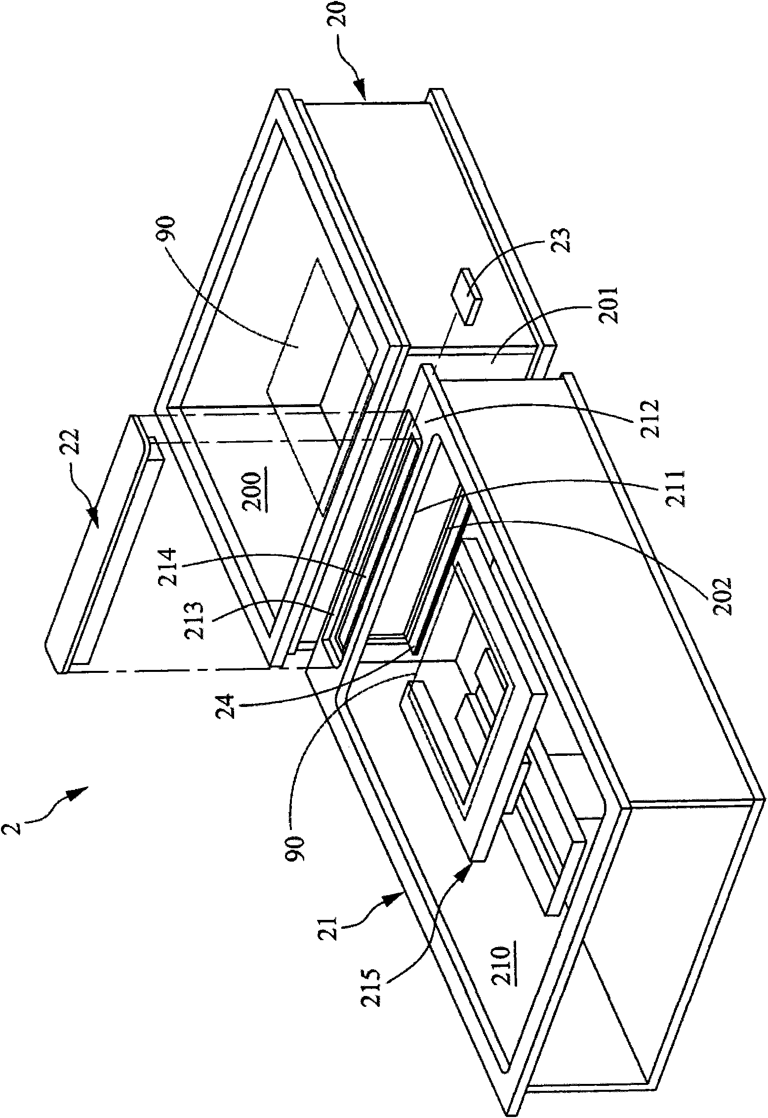
[0071] see Figure 1AAs shown, this figure is a schematic perspective view of an embodiment of the surface treatment device of the present invention. The surface treatment device 2 includes a process chamber 20 , a transmission chamber 21 , a plasma generating device 22 and a control unit 23 . The process chamber 20 has a process space 200 therein to accommodate a substrate 90, and the process chamber 20 can provide a deposition process, so that the substrate 90 in the process chamber 20 is formed as Figure 1B A deposited layer 91 is shown. In this embodiment, the depositi...


PUM


Abstract

The invention provides a surface treatment device and a method thereof. The surface treatment device comprises a process cavity, a transmission cavity and a plasma body generation device, wherein the process cavity provides a deposition manufacture process, the transmission cavity is coupled at one side of the process cavity, an open groove is arranged on the transmission cavity for accommodating the plasma body generation device, and the plasma body generation device generates plasma bodies and guides the plasma bodies into the transmission cavity. The surface treatment device is utilized, the invention also provides a surface treatment method, and after a base plate completes the deposition manufacture process in the process cavity, the plasma body generation device generates the plasma bodies for carrying out surface flattening treatment on deposition layers in the process that the base plate enters the transmission cavity from the process cavity.

Description

technical field [0001] The invention relates to a surface treatment device, in particular to a surface treatment device and a method thereof which use plasma to planarize a deposition layer. Background technique [0002] In the existing thin film manufacturing process, a plasma generating device is placed in the transmission chamber and the process chamber. Before the substrate is transferred to the process chamber, surface cleaning, dry etching, surface activation or modification and other manufacturing processes are performed immediately during the transfer. [0003] For example, when a zinc oxide (ZnO) film is deposited in a low pressure chemical vapor deposition (LPCVD) manufacturing process, since the surface morphology of the zinc oxide film is often pyramid-shaped, a sharp film surface is formed, so it will It affects the coverage and density of the interface, which is not conducive to the fabrication of subsequent element fabrication processes, such as the fabricati...

Claims


Application Information

Patent Timeline
IPC IPC(8): H01L21/00
Inventor 简荣祯杨宏仁张志振林士钦梁沐旺
Owner IND TECH RES INST
Why Eureka
Try Eureka