Package of shape memory alloy core structure

A technology of memory alloy and core structure, which is applied in the direction of electrical components, semiconductor devices, electric solid devices, etc., can solve the problems of package failure and other problems, and achieve the effect of solving failure and improving heat dissipation performance

Inactive Publication Date: 2012-01-25
SAMSUNG SEMICON CHINA RES & DEV +1
View PDF4 Cites 14 Cited by
  • Summary
  • Abstract
  • Description
  • Claims
  • Application Information

AI Technical Summary

Problems solved by technology

[0007] However, for thinner packages or PoP packages, a series of high-temperature reflow processes are required during the manufacturing process. Part of the material in the package will be defor

Method used


Image

  • Package of shape memory alloy core structure
  • Package of shape memory alloy core structure
  • Package of shape memory alloy core structure

Examples


Embodiment Construction

[0024] Hereinafter, exemplary embodiments of the present invention will be described in detail with reference to the accompanying drawings. This invention may, however, be embodied in many different forms and should not be limited to the exemplary embodiments set forth herein. Rather, these exemplary embodiments are provided so that this disclosure will be thorough and complete, and will fully convey the scope of the exemplary embodiments to those skilled in the art. The size and relative sizes of layers and regions may be exaggerated in the drawings for clarity. Also, in the drawings, the same or similar reference numerals may denote the same or similar elements.

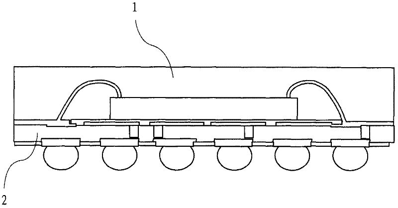
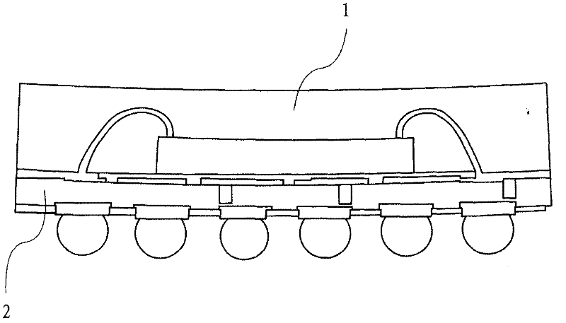
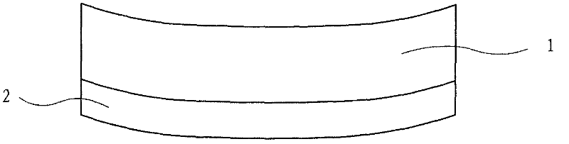
[0025] figure 1 is a schematic diagram showing a package according to the prior art.

[0026] refer to figure 1 , the package according to the prior art may include: a substrate 2; a chip on the substrate 2; solder balls formed under the substrate, wherein the substrate may be, for example, a PCB, and the chip ...


PUM

PropertyMeasurementUnit
Deformation temperatureaaaaaaaaaa

Abstract

The invention provides a package of a shape memory alloy core structure, comprising a substrate, a chip arranged on the substrate, a plastic package material used for packing the chip on the substrate and a shape memory alloy embedded in the substrate. The package with the shape memory alloy embedded in the substrate improves the heat dispersion; due to the deformation of the shape memory alloy in the process of high temperature backflow in a packaging technology, the package can control the deformation direction to be opposite to the deformation directions of the substrate [such as a PCB (printed circuit board)] and the plastic package, thus at least partially restraining and/or offsetting the deformation of the substrate (such as the PCB) at a high temperature, and solving the problem of the packaging structure failure due to the deformation of the substrate and the plastic package at the high temperature.

Description

technical field [0001] The invention relates to a package of shape memory alloy core structure. In particular, the present invention relates to a package containing a shape memory alloy embedded in a substrate such as a printed circuit board (PCB). Background technique [0002] With the rapid development of the semiconductor industry and its rapid penetration into various industries, electronic packaging has gradually become a bottleneck in the realization of the functions of semiconductor chips. Therefore, electronic packaging has achieved tremendous development in the past 20 to 30 years, and has made considerable progress. progress. [0003] Today's electronic packaging must not only provide chip protection, but also meet increasing functions, reliability, and heat dissipation while controlling costs. The design and manufacture of electronic packaging is becoming more and more important to system applications. The design and manufacture of electronic packaging needs to ...

Claims


Application Information

Patent Timeline
IPC IPC(8): H01L23/14H01L23/28H01L23/373
CPCH01L2224/32225H01L2924/3511H01L2224/48227H01L2924/15311H01L2224/73265H01L24/73H01L2924/00012H01L2924/00
Inventor 马慧舒杜茂华
Owner SAMSUNG SEMICON CHINA RES & DEV
Why Eureka
Try Eureka