Gallium nitride transistor for AC/DC and manufacturing method thereof

A transistor and gallium nitride technology, applied in the field of AC/DC gallium nitride transistors and their manufacturing, can solve the problems affecting the performance and service life of gallium nitride transistors, the poor heat dissipation performance of gallium nitride transistors, and the increase of gallium nitride transistors. Transistor cost and other issues, to achieve the effect of optimizing performance and service life, strong practicability, and reducing loss and impact

Inactive Publication Date: 2021-04-16
令储(上海)科技发展有限公司
View PDF0 Cites 0 Cited by
  • Summary
  • Abstract
  • Description
  • Claims
  • Application Information

AI Technical Summary

Problems solved by technology

[0004] The purpose of the present invention is to provide a gallium nitride transistor for AC/DC and its manufacturing method in order to solve the above problems, which solves the problem that the heat dissipation performance of the current gallium nitride tr

Method used


Image

  • Gallium nitride transistor for AC/DC and manufacturing method thereof
  • Gallium nitride transistor for AC/DC and manufacturing method thereof
  • Gallium nitride transistor for AC/DC and manufacturing method thereof

Examples


Example Embodiment

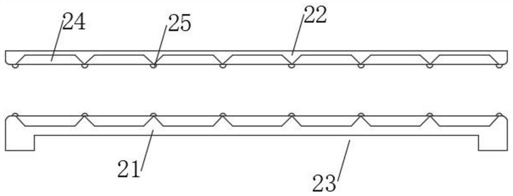
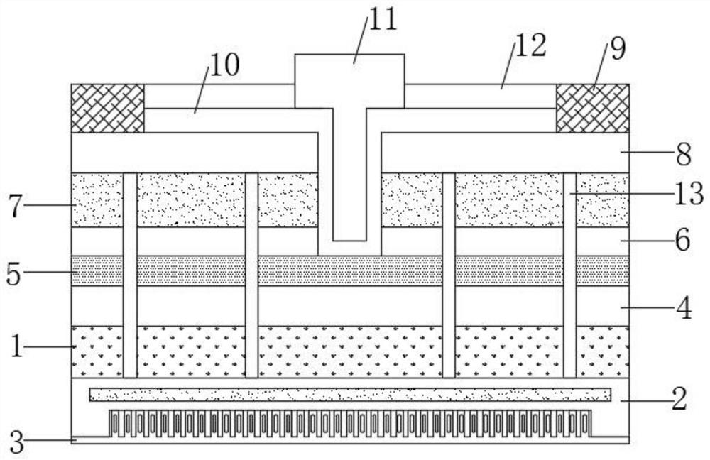
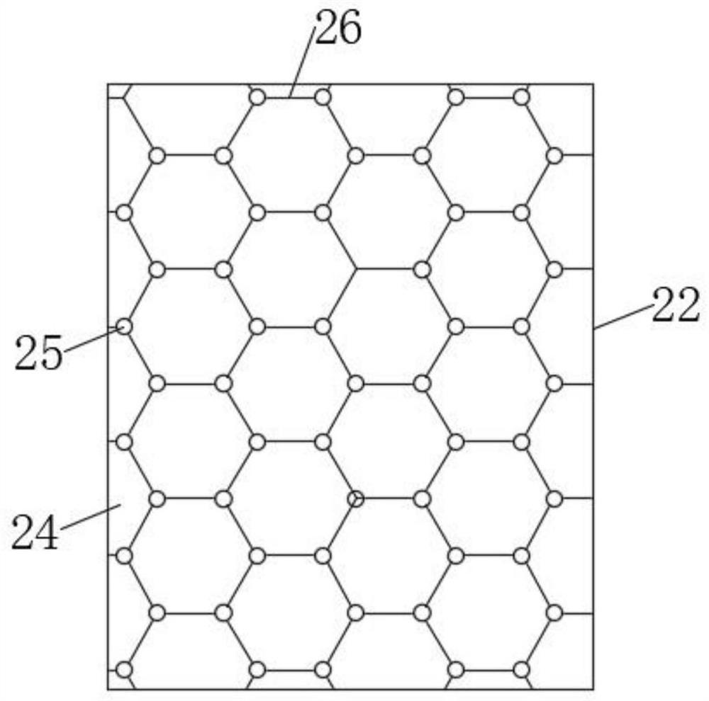
[0026] like Figure 1-4 As shown, this specific embodiment adopts the following technical solution: a gallium nitride transistor for AC / DC, including a nucleation layer 1 and a substrate layer 2, the bottom of the nucleation layer 1 is provided with a substrate layer 2, so The substrate layer 2 is provided with a fluid heat dissipation structure, the bottom of the substrate layer 2 is fixedly installed with a heat sink 3, and the top of the nucleation layer 1 is provided with a conductive buffer layer 4, and the conductive buffer layer 4 is far away from the nucleation layer. One side of 1 is provided with a drift layer 5, and the side of the drift layer 5 away from the conductive buffer layer 4 is provided with an electron blocking layer 6, and the side of the electron blocking layer 6 away from the conductive buffer layer 4 is provided with a channel layer 7 , the side of the channel layer 7 away from the electron blocking layer 6 is provided with a barrier layer 8, and the ...


PUM


Abstract

The invention discloses a GaN transistor for AC/DC and manufacturing method thereof. The GaN transistor comprises a nucleating layer and a substrate layer; the substrate layer is arranged at the bottom of the nucleating layer, a fluid heat dissipation structure is arranged on the substrate layer, a heat dissipation base is fixedly mounted at the bottom of the substrate layer, a conductive buffer layer is arranged at the top of the nucleating layer, and a drift layer is arranged on the side, away from the nucleating layer, of the conductive buffer layer; an electron blocking layer is arranged on the side, away from the conductive buffer layer, of the drift layer; a channel layer is arranged on the side, away from the conductive buffer layer, of the electron blocking layer; a barrier layer is arranged on the side, away from the electron blocking layer, of the channel layer, and source electrodes are arranged on the two opposite sides of the top of the barrier layer. The GaN transistor has the beneficial effects that the fluid heat dissipation structure is arranged on the substrate layer; the substrate layer is good in heat dissipation performance, and the heat dissipation seat is mounted on the lower substrate layer, so that the gallium nitride transistor is integrally provided with a heat dissipation structure, with the added fluid heat dissipation structure and the heat dissipation seat, the heat dissipation performance of the gallium nitride transistor is effectively improved, the use performance of the gallium nitride transistor is optimized, the service life of the gallium nitride transistor is prolonged, and the cost is reduced.

Description

Technical field: [0001] The invention belongs to the technical field of gallium nitride transistors, in particular to a gallium nitride transistor for AC / DC and a manufacturing method thereof. Background technique: [0002] For the first time, French and Swiss scientists used gallium nitride on a (100)-silicon (crystal orientation of 100) base to successfully manufacture high-performance high-electron mobility transistors, which grow on the top of the substrate layer to form a nucleation layer. The top of the nuclear layer forms a conductive buffer layer, the top of the conductive buffer layer forms a drift layer, the top of the drift layer forms an electron blocking layer, the top of the electron blocking layer forms a channel layer, and the top of the channel layer forms a dielectric layer and a source electrode, A gate electrode diamond layer is formed on the dielectric layer, so as to obtain a gallium nitride transistor functional region structure. [0003] At present, ...

Claims


Application Information

Patent Timeline
IPC IPC(8): H01L29/778H01L23/367H01L21/335
Inventor 鲍通
Owner 令储(上海)科技发展有限公司
Why Eureka
Try Eureka