Low-congestion communication method and router for realizing shared path transmission of optical network on chip

A network-on-optical-chip and shared path technology, which is applied in the field of low-blocking communication methods and routers, can solve the problems of low overhead and energy consumption, network congestion, and low utilization of optical links, etc. The effect of controlling expenses

Inactive Publication Date: 2012-01-25
XIDIAN UNIV
View PDF2 Cites 16 Cited by
  • Summary
  • Abstract
  • Description
  • Claims
  • Application Information

AI Technical Summary

Problems solved by technology

[0005] The purpose of the present invention is to overcome the deficiencies of the above-mentioned prior art, and propose a low-blocking communication method and router for realizing the shared path transmission of the network on the optical chip, so as to solve the problem of low utilization rate of optical links and serious network congestion in the Mesh structure of the network on the optical chip problems, to ensure low network overhead and energy consumption, and to improve network throughput and performance

Method used


Image

  • Low-congestion communication method and router for realizing shared path transmission of optical network on chip
  • Low-congestion communication method and router for realizing shared path transmission of optical network on chip
  • Low-congestion communication method and router for realizing shared path transmission of optical network on chip

Examples


Embodiment 1

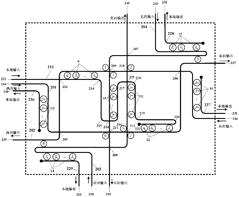
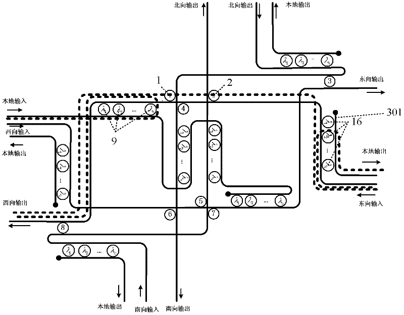
[0087] refer to image 3 , on-chip optical signal group G 1 Enter the router from the east to the input port along the path shown by the dotted line in the figure. At this time, the on-chip optical signal group G 1 including communication wavelength λ 1 The optical signal and communication wavelength is λ 2 optical signal, the on-chip optical signal group is first transmitted along the optical waveguide, and when it reaches the position of the narrowband microring resonator group 16, since the resonance wavelength is λ 2 The narrowband microring is in the open state, and the on-chip optical signal group G 1 The medium wavelength is λ 2 The optical signal is diverted and coupled to another waveguide 301 for transmission. At this time, the optical signal group G 1 The remaining wavelength in λ is 1 The optical signal of , since the broadband microring resonators 2 and 4 are both in the off state, the wavelength is λ 1 The optical signal is transmitted along the original w...

Embodiment 2

[0089] refer to Figure 4 , two waveguides 402 and 403 cross to form a crossing point, and the broadband microring resonator 401 is located on one side of the waveguide crossing point; Figure 4 (a) is a schematic diagram of the transmission of the on-chip optical signal group through the broadband microring resonator in the off state. When the broadband microring resonator 401 is in the off state, the on-chip optical signal group is transmitted along the original optical waveguide; Figure 4 (b) is a schematic diagram of the transmission of the on-chip optical signal group through the broadband microring resonator in the on-state. When the broadband micro-ring resonator 401 is in the on-state, the on-chip optical signal group turns 90 degrees and is coupled to another optical waveguide for transmission. .

Embodiment 3

[0091] refer to Figure 5 , the broadband microring resonator 501 is located in the parallel interval of the waveguides 502 and 503; Figure 5 (a) is a schematic diagram of the transmission of the on-chip optical signal group through the broadband microring resonator in the off state. When the broadband microring resonator 501 is in the off state, the on-chip optical signal group is transmitted along the original optical waveguide; Figure 5 (b) is a schematic diagram of the transmission of the on-chip optical signal group through the broadband microring resonator in the on-state. When the broadband micro-ring resonator 501 is in the on-state, the on-chip optical signal group turns 180 degrees and is coupled to another optical waveguide for transmission. .


PUM


Abstract

The invention discloses a low-congestion communication method and a router for realizing the shared path transmission of an optical network on chip. By the method and the router, the problem of serious network congestion caused by single wavelength communication in the Mesh structure of the conventional optical network on chip is mainly solved. The router provided by the invention comprises optical waveguides, broadband micro-ring resonators and narrowband micro-ring resonator groups, and is used for constructing an optical transmission network of a network on chip. In the communication method, the shared path transmission of a plurality of pairs of communication nodes is realized by utilizing a wavelength division multiplexing technology; judgment in path sharing and the allocation of wavelengths are executed by utilizing a conventional electric control network; when a link establishment packet is congested by the locking of an output port, the judgment in the path sharing may be executed, available wavelengths are allocated for the link establishment packet capable of sharing a path, and then the link establishment packet is continuously forwarded and a plurality of data packets perform the shared optical path transmission by using different communication wavelengths. By the method and the router, the multi-wavelength communication of the Mesh structure of the network on chip can be effectively supported, network congestion can be reduced, network overhead can be decreased and network performance can be improved.

Description

technical field [0001] The invention belongs to the technical field of communication, and relates to a low-blocking communication method and a router in an Optical-Network-On-Chip communication system, which are used to determine the communication mode between IP cores and the construction of an optical communication network. Background technique [0002] With the development of VLSI technology, the size of electronic components will be further reduced, and the operating frequency of chips will be increased to GHz or even higher. At this time, the traditional electrical interconnection architecture adopted by the network on chip will have obvious technical bottlenecks such as parasitic effects, electromagnetic interference, signal delay, etc. These problems will seriously limit the working bandwidth of the electrical interconnection network on chip. At the same time, the energy consumption of the electrical interconnection framework has also become the focus of researchers. ...

Claims


Application Information

Patent Timeline
Patent Type & Authority Applications(China)
IPC IPC(8): H04Q11/00H04L12/56H04L12/801
Inventor 顾华玺余晓杉杨银堂王琨白露莹
Owner XIDIAN UNIV
Why Eureka
Try Eureka