AI technical title is built by PatSnap AI team. It summarizes the technical point description of the patent document.
A processing method and write balancing technology, which is applied in the direction of memory address/allocation/relocation, etc., can solve the problems of reduced read and write performance, and achieve high read performance
Active Publication Date: 2012-02-01
ANYKA (GUANGZHOU) MICROELECTRONICS TECH CO LTD
View PDF4 Cites 9 Cited by
Summary
Abstract
Description
Claims
Application Information
AI Technical Summary
This helps you quickly interpret patents by identifying the three key elements:
Problems solved by technology
Method used
Benefits of technology
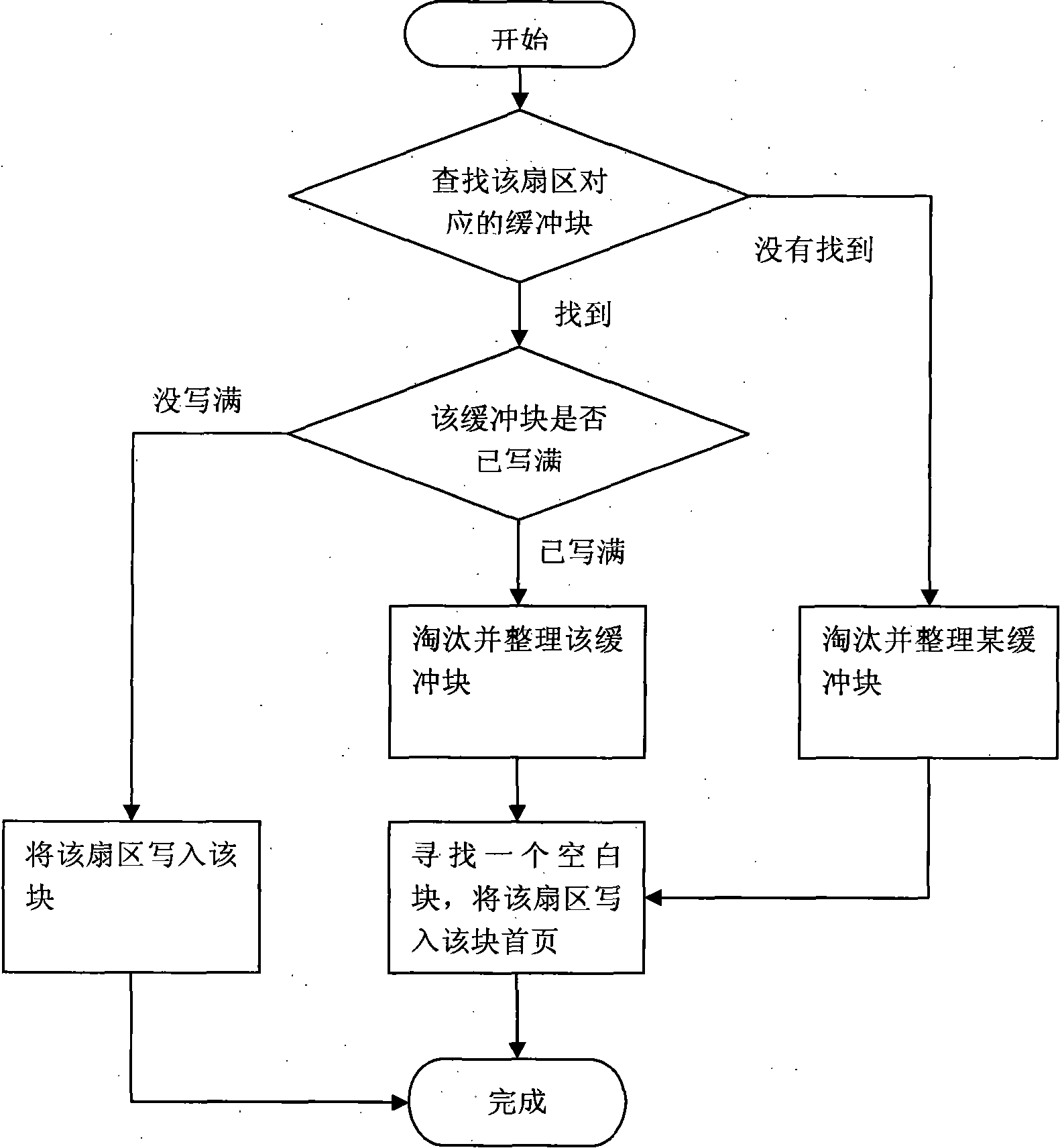
Problems solved by technology
Therefore, when a certain sector is updated, the entire physical block corresponding to it will be updated at the same time, and the read and write performance will be greatly reduced relatively.
Method used
Image
Click on the blue label to locate the original text in one second.
Reading with bidirectional positioning of images and text.
Examples
specific Embodiment approach 1
[0029] Specific implementation mode 1: Simulator implementation mode
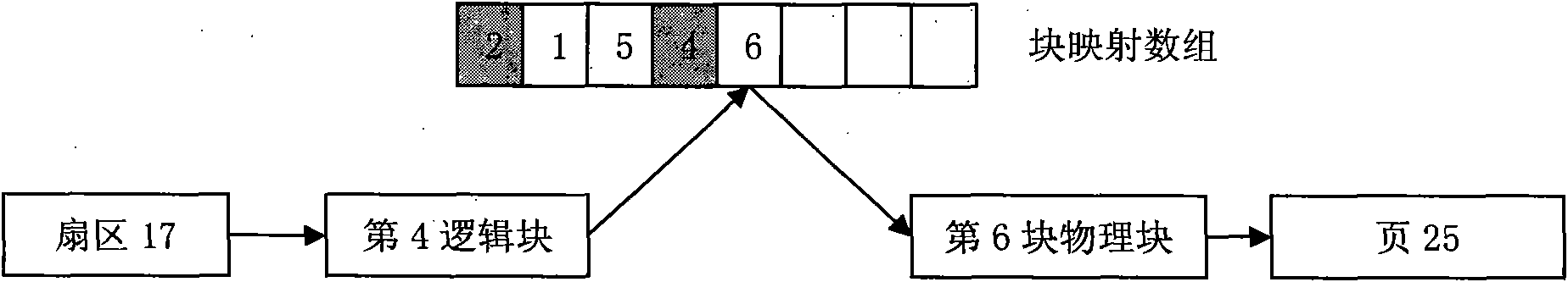
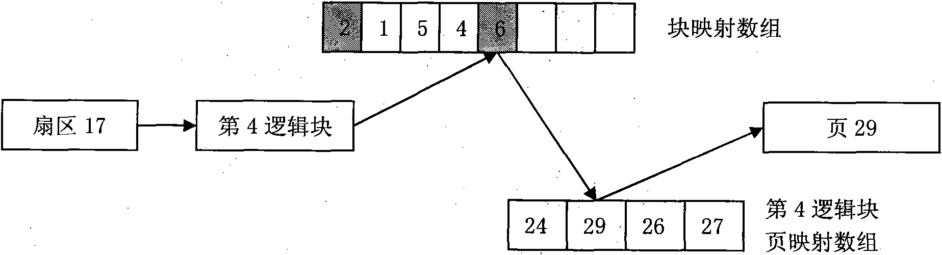
[0030] The simulation environment is: the total number of blocks of Nand Flash is 8, each block has 4 pages, and each page is 2K bytes; the write buffer block has 2 physical blocks; the block starts with number 0, and the number of the first page in the block is also 0.
[0031] The initialization operation process is as follows:
[0032] 1) Allocate the memory used by 1 block mapping array and 2 page mapping arrays.
[0033] 2) Scan all physical blocks of the Nand chip, update the block mapping array, and reproduce the block mapping relationship. The possible mapping relationship is as follows figure 2 .
[0034] 3) For the buffer block, scan each page, update the page mapping array, and reproduce the page mapping relationship. The possible mapping relationship is as follows image 3 .
[0035] For read operations, use the figure 2 The mapping transformation shown. Suppose you want to read 17 secto...
specific Embodiment approach 2
[0038] Specific implementation mode two: real hardware implementation mode
[0039] This method is realized in the WinCE operating system. As an example of product quality level, this method sets the number of buffer blocks to 16 or higher, adds power-off processing and dynamic bad block management, and makes a lot of optimizations. The various operations of this example are as follows:
[0040] 1) Initialization operation:
[0041] a) Allocate the memory used by the block mapping array and the N page mapping arrays.
[0042] b) Scan all physical blocks of the Nand chip, update the block mapping array, and reproduce the block mapping relationship.
[0043] c) For the buffer block, scan each page, update the page mapping array, and reproduce the page mapping relationship.
[0044] 2) Read sector operation:
[0045] a) Calculate the logic block.
[0046]b) Find the corresponding physical block according to the block mapping array.
[0047] c) If the logic block is in the ...
PUM
Abstract
The invention discloses a Nand writing balance processing method which comprises the following operating processes: (1) a certain logic block is in a buffer state, the logic block corresponds to two physical blocks, wherein the first physical block is used as an old data block to be read in firstly; a page mapping relationship between the logic block and the first physical block is one-to-one mapping; the second physical block is used as a buffer block to be read in later, and a page mapping relationship between the logic block and the second physical block is random mapping; (2) according to a write bufferalgorithm, the page mapping relationship is established; (3) in the write operation process of the physical blocks, if the buffer block which corresponds to the physical block is overwritten, the housekeeping operation process is triggered; the write operation on the physical operation is finished; meanwhile, the corresponding relationship between the logic block and the buffer block is released. According to the Nand writing balance processing method, the two algorithms of page mapping and block mapping are combined so that the high efficiency of read-write performance is ensured while the occupied memory is substantially reduced.
Description
technical field [0001] The invention relates to a Nand write balance processing method. Background technique [0002] A Nand Flash chip is composed of many blocks (Blocks), and a block is composed of many pages (Pages). Each block or page has a certain number of erases and writes. Therefore, the easiest way to extend the service life of Nand Flash is to write balance. . Write balance, the English word is Wear-leveling, that is, trying to make each block have the same number of erasures, and each page has the same number of writes. Therefore, the sectors of the file system must be mapped to different physical pages in a certain way. Write balance algorithm is a basic research topic, the most important content of which is the mapping relationship. According to the mapping relationship, the current popular write balancing algorithms can be divided into two categories: page mapping and block mapping. [0003] Page mapping algorithm: through an array in memory, establish the ...
Claims
Application Information
Patent Timeline
Application Date:The date an application was filed.
Publication Date:The date a patent or application was officially published.
First Publication Date:The earliest publication date of a patent with the same application number.
Issue Date:Publication date of the patent grant document.
PCT Entry Date:The Entry date of PCT National Phase.
Estimated Expiry Date:The statutory expiry date of a patent right according to the Patent Law, and it is the longest term of protection that the patent right can achieve without the termination of the patent right due to other reasons(Term extension factor has been taken into account ).
Invalid Date:Actual expiry date is based on effective date or publication date of legal transaction data of invalid patent.
IPC IPC(8): G06F12/06
Inventor李晓辉胡胜发
OwnerANYKA (GUANGZHOU) MICROELECTRONICS TECH CO LTD

