Substrate cleaning apparatus, coating and developing apparatus having the same and substrate cleaning method

一种清洗装置、基板的技术,应用在清洁方法和用具、化学仪器和方法、摄影等方向,能够解决制造成本上升、涂覆显影装置占有面积变大、半导体集成电路制造成本上升等问题,达到节省空间的效果

Active Publication Date: 2012-02-01
TOKYO ELECTRON LTD
View PDF5 Cites 6 Cited by
  • Summary
  • Abstract
  • Description
  • Claims
  • Application Information

AI Technical Summary

Problems solved by technology

[0006] However, in the case where the chamfering grinding mechanism is provided in the substrate cleaning unit as described above, since a space for installing the chamfering grinding mechanism is required in the substrate cleaning unit, the substrate cleaning unit tends to be enlarged.
Therefore, the occupied area of ​​the coating and developing device having the substrate cleaning unit also becomes larger.
In addition, since the operation of the chamfering and grinding mechanism requires a predetermined time, it leads to a decrease in the manufacturing productivity of semiconductor integrated circuits and the like.
In addition, since the manufacturing cost of the chamfering and grinding mechanism is required, the manufacturing cost of the substrate cleaning unit and the coating and developing device having the substrate cleaning unit increase, which in turn leads to an increase in the manufacturing cost of semiconductor integrated circuits and the like.

Method used


Image

  • Substrate cleaning apparatus, coating and developing apparatus having the same and substrate cleaning method
  • Substrate cleaning apparatus, coating and developing apparatus having the same and substrate cleaning method
  • Substrate cleaning apparatus, coating and developing apparatus having the same and substrate cleaning method

Examples


Embodiment 1

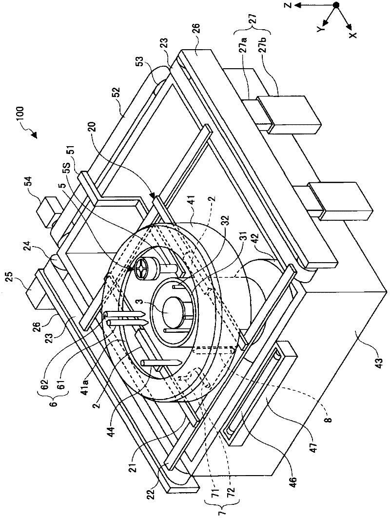
[0099] The chamfered portion of the experimental wafer was cleaned in the substrate cleaning apparatus 100 having the cleaning head 5 .

Embodiment 2

[0101] A brush made of bundled plastic fibers was used instead of a PVA sponge, and a cleaning nozzle 5 (described later) was installed in the substrate cleaning device 100 , and the chamfer of the experimental wafer was cleaned using the substrate cleaning device 100 department.

[0102] refer to Figure 13It can be seen that only about 42% of shavings were removed when the brush of the comparative example was used. It can be considered that such a removal rate is due to the fact that the brush of the comparative example does not have the central portion 5a and the ring portion 5b, and that the brush of the comparative example does not contact (or rub) the chamfer of the experimental wafer.

[0103] When the cleaning liquid was sprayed from the cleaning nozzle to the chamfered portion, about 47% of the shavings adhering to the chamfered portion were removed, and the removal rate was higher than that of the brush of the comparative example. However, since the cleaning using ...


PUM


Abstract

The present disclosure relates to a substrate cleaning apparatus, a coating and developing apparatus and a substrate cleaning method. The space-saving substrate cleaning apparatus is capable of cleaning a beveled portion easily and efficiently. The substrate cleaning apparatus in the embodiment includes a substrate holding and rotating unit for holding a center of a rear surface of a substrate and rotating the substrate; a cleaning unit including a first cleaning member, a second cleaning member provided around the first cleaning member and a base to which the first and second cleaning members are secured; an elevating unit for moving the substrate holding and rotating unit and the cleaning unit relative to each other so as to allow the first and second cleaning members to come into contact with the rear surface of the substrate held by the substrate holding and rotating unit; and a driving unit for driving the substrate and the cleaning unit relative to each other in a direction along the rear surface of the substrate so as to allow part of the second cleaning member to be exposed to the outside of the substrate.

Description

technical field [0001] The present invention relates to a substrate cleaning device for cleaning substrates such as semiconductor wafers and flat panel display glass substrates (FPD substrates), a coating and developing device having the substrate cleaning device, and a substrate cleaning method. Background technique [0002] In the manufacturing process of semiconductor integrated circuits and FPDs, photolithography is indispensable for forming a photoresist pattern used as an etching mask on a substrate. In photolithography, specifically, a photoresist film is formed by coating a photoresist liquid on a substrate such as a semiconductor wafer or an FPD substrate, and a photomask (mask) with a predetermined pattern is used. mold) to expose the photoresist film, and develop the exposed photoresist film to form a photoresist pattern. For such processing, a photoresist pattern forming system configured by connecting an exposure device to a coating and developing device for co...

Claims


Application Information

Patent Timeline
Patent Type & Authority Applications(China)
IPC IPC(8): H01L21/67H01L21/02B08B11/04G03F7/00
CPCH01L21/02087H01L21/67051H01L21/02052H01L21/0273H01L21/68742H01L21/68764
Inventor 大河内厚久米纯次
Owner TOKYO ELECTRON LTD
Why Eureka
Try Eureka