Semiconductor structure and manufacturing method thereof

A technology of semiconductor and laminated structure, applied in the direction of semiconductor/solid-state device manufacturing, semiconductor device, semiconductor/solid-state device components, etc., can solve problems such as short circuits, and achieve the effect of avoiding short circuits and improving yield.

Inactive Publication Date: 2012-02-01
INST OF MICROELECTRONICS CHINESE ACAD OF SCI
View PDF5 Cites 15 Cited by
  • Summary
  • Abstract
  • Description
  • Claims
  • Application Information

AI Technical Summary

Problems solved by technology

[0004] However, for figure 1 The self-aligned via stack structure shown can still cause short circuit problems due to the inability to freely change the via size

Method used


Image

  • Semiconductor structure and manufacturing method thereof
  • Semiconductor structure and manufacturing method thereof
  • Semiconductor structure and manufacturing method thereof

Examples


Embodiment Construction

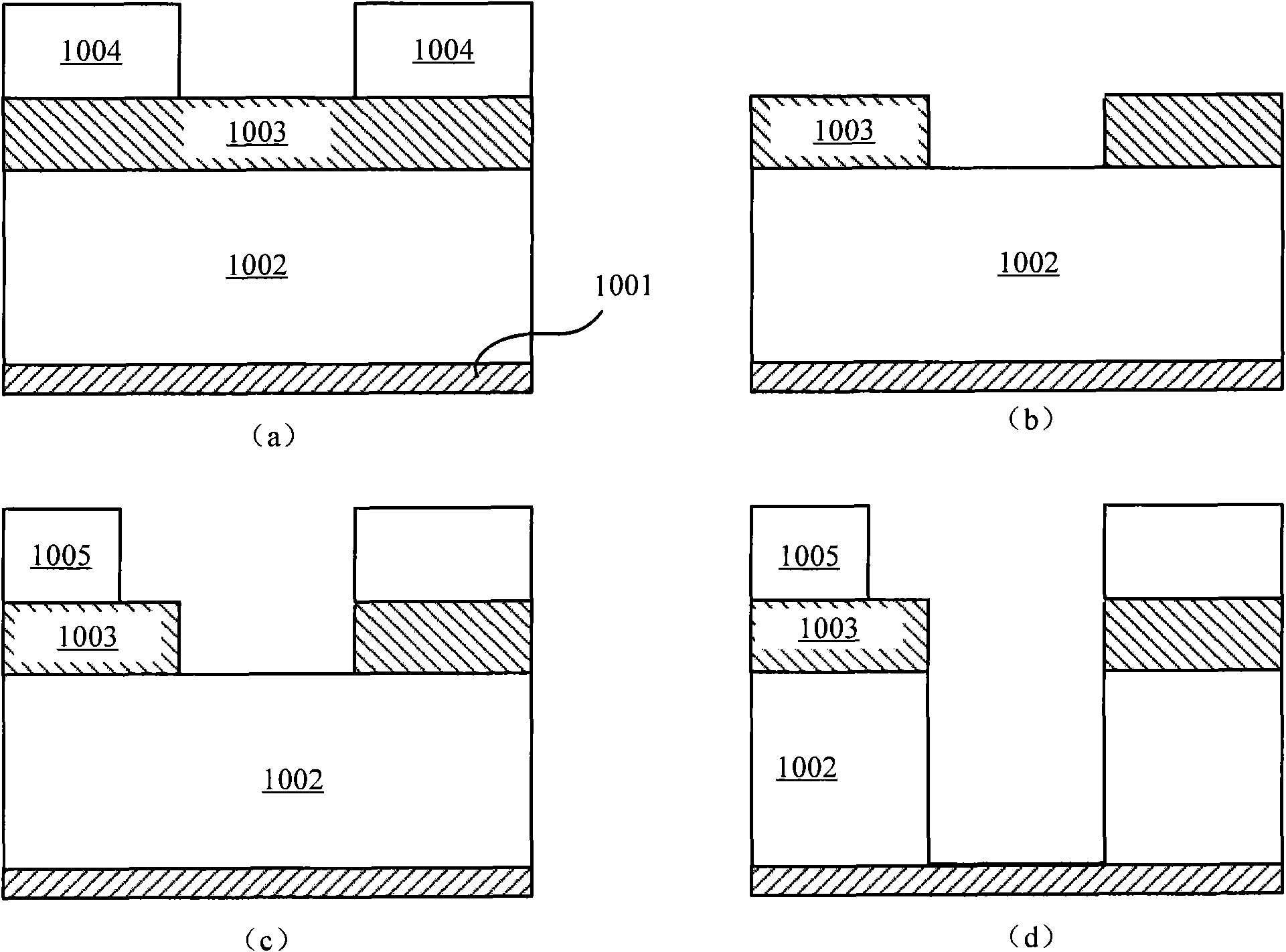
[0024] The preferred embodiments of the present invention will be described in detail below with reference to the accompanying drawings, and unnecessary details and functions for the present invention will be omitted during the description to avoid confusing the understanding of the present invention.

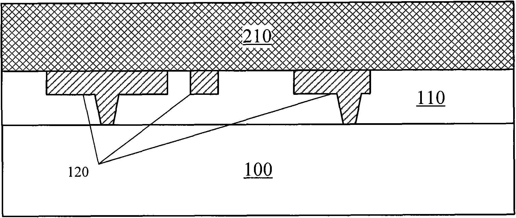
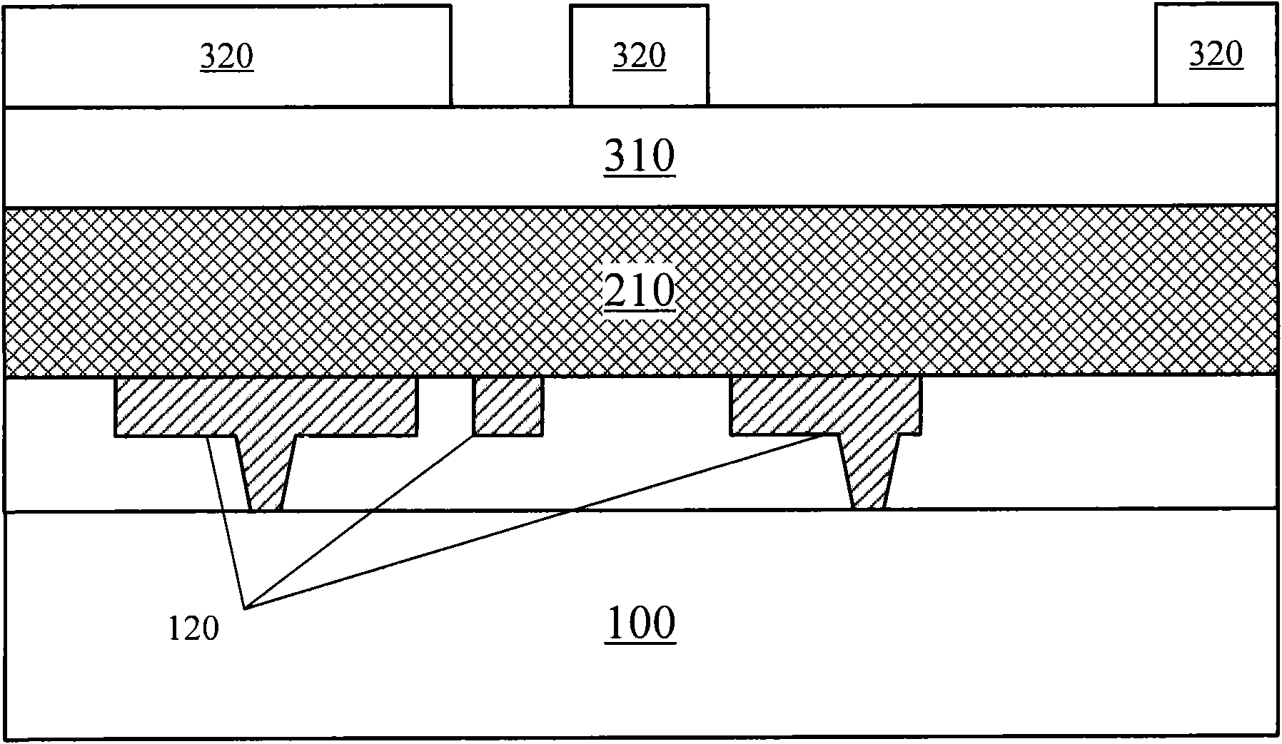
[0025] First, refer to Figure 11-12 , to describe in detail the semiconductor structure manufactured according to the process proposed in the first embodiment of the present invention. Figure 11 A schematic diagram of a semiconductor structure manufactured by the semiconductor structure manufacturing method proposed according to the first embodiment of the present invention is shown.

[0026] Such as Figure 11 As shown, the semiconductor structure manufactured according to the process proposed in the present invention mainly includes: a semiconductor substrate 100, a first dielectric layer 110 formed on the semiconductor substrate 100, a second dielectric layer 210 formed o...


PUM

PropertyMeasurementUnit
Thicknessaaaaaaaaaa
Bottom widthaaaaaaaaaa

Abstract

The invention discloses a semiconductor structure and a manufacturing method thereof. The semiconductor structure comprises a semiconductor substrate, a local-interconnection structure connected with the semiconductor substrate and a via stack structure electrically connected with the local-interconnection structure, wherein the via stack structure comprises a via, a via side wall, an insulating layer and a conductive plug; the via comprises an upper via and a lower via; the width of the upper via is wider than that of the lower via; the via side wall is formed close to the internal wall of the lower via; the insulating layer is formed to cover the surfaces of the via and the via side wall; and the conductive plug is formed in a space encircled by the insulating layer and is electrically connected with the local-interconnection structure. The semiconductor structure and the manufacturing method thereof disclosed by the invention are suitable for the manufacture of via stacks in semiconductor manufacture.

Description

technical field [0001] The present invention relates to the field of semiconductors, in particular to semiconductor structures and fabrication methods thereof, and more particularly to a method for fabricating self-aligned via stacks with variable via sizes and fabrication of via stacks using the method A semiconductor structure with variable via size self-aligned via stacks. Background technique [0002] With the reduction of the mutual spacing of semiconductor devices, the metal connection above the via hole leads to the increase of via-via short circuit problem, so the via-metal line in the photolithography process Higher wiring alignment requirements lead to higher manufacturing costs for mass production. Another approach is to make smaller vias, but this further increases the photolithographic requirements. [0003] There is currently a self-aligned method for manufacturing via stacks, which can simultaneously form vias and metal interconnections. The simultaneous fo...

Claims


Application Information

Patent Timeline
IPC IPC(8): H01L23/528H01L21/768
CPCH01L21/76811H01L23/5329H01L21/76832H01L21/76834H01L21/76804H01L21/76813H01L2924/0002H01L2924/00
Inventor 朱慧珑尹海洲骆志炯
Owner INST OF MICROELECTRONICS CHINESE ACAD OF SCI
Why Eureka
Try Eureka