
Method for making single-sided circuit board with flat wires arranged side by side

A circuit board, single-sided technology, applied in the direction of assembling printed circuits with electrical components, printed circuits connected with non-printed electrical components, printed circuits, etc., can solve the problems of high cost, low efficiency, serious pollution, etc. simple effect

Active Publication Date: 2012-02-01
TONGLING GUOZHAN ELECTRONICS
View PDF3 Cites 37 Cited by
  • Summary
  • Abstract
  • Description
  • Claims
  • Application Information

AI Technical Summary

Problems solved by technology

However, the former is costly and polluting, while the latter is too inefficient to be mass-produced

Method used

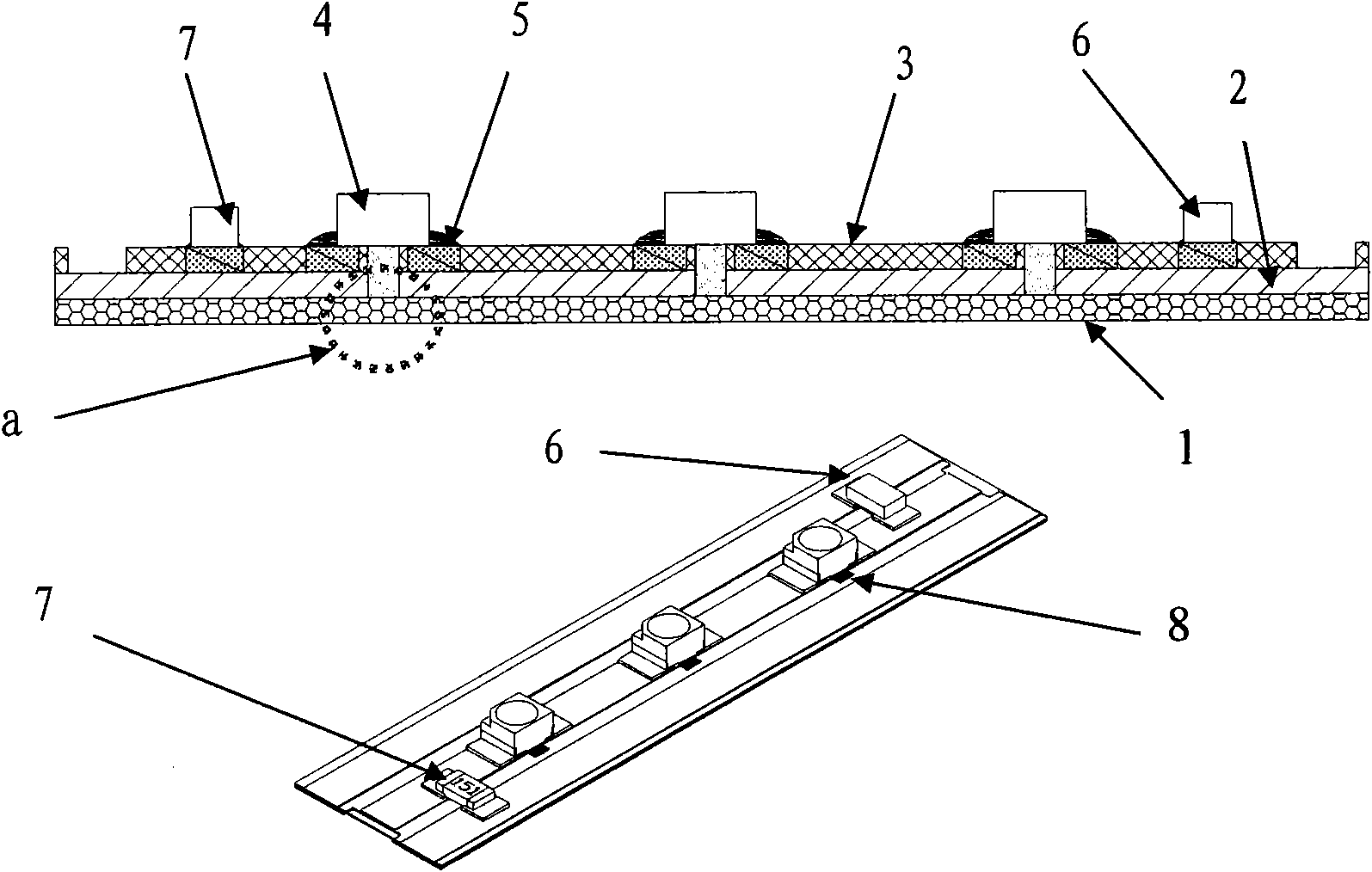
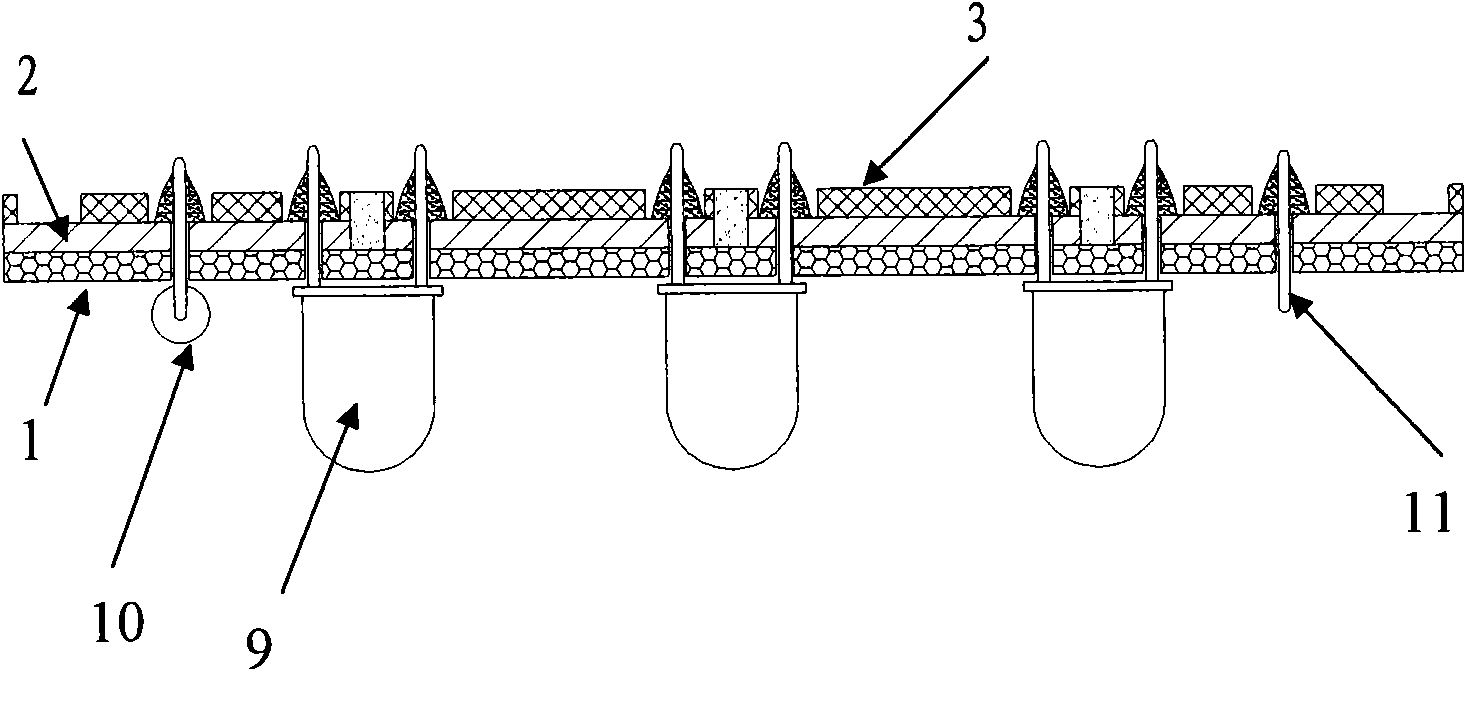

Image

  • Method for making single-sided circuit board with flat wires arranged side by side
  • Method for making single-sided circuit board with flat wires arranged side by side
  • Method for making single-sided circuit board with flat wires arranged side by side

Examples


Embodiment Construction

[0046] A specific embodiment of a method for manufacturing a single-sided circuit board by juxtaposing flat wires according to the present invention will be described in more detail below.

[0047] However, those skilled in the art should understand that the following are only examples and descriptions of some preferred implementations, and other similar or equivalent implementations can also be used to implement the present invention.

[0048] (1) Fabrication of rigid circuit board

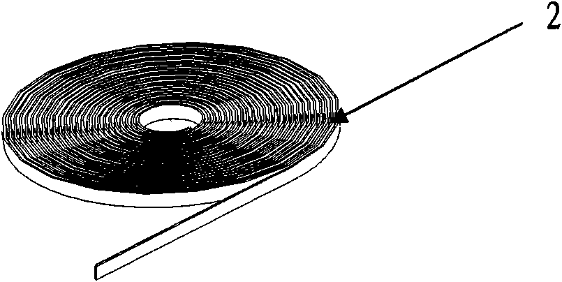
[0049] 1. The production of flat wires is made by cutting copper foil into strips or rolling copper wires or flat wires of a certain width and thickness with a flat wire calender 2 (such as image 3 ).

[0050] 2. Fabrication of juxtaposition groove molds: process juxtaposition grooves 12 consistent with the line width by using a mirror surface stainless steel plate by etching or mechanical processing (such as Figure 4 shown), the depth of the groove 12 is shallower than the thickness of the f...


PUM


Abstract

The invention relates to a method for making a single-sided circuit board with flat wires arranged side by side. Specifically, according to one aspect of the invention, after a covering film provided with a solder pad window is directly glued with flat wires arranged side by side through hot pressing, parts of the wries, which need to be disconnected are cut off, and then the flat wires are simultaneously pressed on a substrate of the circuit board with a gluing property. Bridging connection is realized through printing electricity conducting ink or soldering conductors. When characters are printed, character ink is printed on the covering film and the cut opening parts of the flat wires for filling the openings, and exposed conductors at the cut opening parts are insulated. When a jack element needs to be arranged, soldering installation can be realized as long as a hole is directly drilled in a soldered spot or a hole is punched by a die. The circuit board can be made without etching. Compared with the traditional circuit board making technology, the novel technology has the advantages of excellent environment friendliness, energy saving and material saving.

Description

technical field [0001] The invention belongs to the circuit board industry. According to one aspect of the present invention, the cover film with the pad window and the juxtaposed flat wire are directly bonded by thermocompression, the position where the flat wire needs to be disconnected is cut off, and then pressed together on the adhesive circuit board base. On the material, the bridge connection is connected by printing conductive ink or soldering conductors. At the same time as printing text, the opening of the cover film and flat wire can be printed with text ink to form filling, and the exposed conductor at the cut off opening can be filled. Insulation treatment. Use this method to make single-sided circuit boards. Make circuit boards without etching. [0002] Compared with the traditional process for making circuit boards, the present invention is a very environmentally friendly, energy-saving and material-saving new technology. Background technique [0003] Trad...

Claims


Application Information

Patent Timeline
IPC IPC(8): H05K3/00H05K3/34H05K1/00H05K1/18F21V23/06F21Y101/02
CPCH05K3/3431H05K2201/1028H05K2201/10106H05K3/321H05K3/3421H05K3/041H05K3/202
Inventor 王定锋徐文红
Owner TONGLING GUOZHAN ELECTRONICS
Learn More