Semiconductor packaging structure with multiple convex block structures

A packaging structure and semiconductor technology, which is applied in the direction of semiconductor devices, semiconductor/solid-state device parts, electric solid-state devices, etc., can solve the problems of semiconductor packaging reliability test, bump increase, etc., and achieve the effect of ensuring reliability and avoiding failure

Inactive Publication Date: 2012-02-22
ADVANCED SEMICON ENG INC
View PDF5 Cites 2 Cited by
  • Summary
  • Abstract
  • Description
  • Claims
  • Application Information

AI Technical Summary

Problems solved by technology

In particular, as the size of the bumps shrinks, the risk of failure of the bumps located at the corners of the component junctions due to stress damage increases significantly, which severely tests the reliability of the semiconductor package.

Method used


Image

  • Semiconductor packaging structure with multiple convex block structures
  • Semiconductor packaging structure with multiple convex block structures
  • Semiconductor packaging structure with multiple convex block structures

Examples


Embodiment Construction

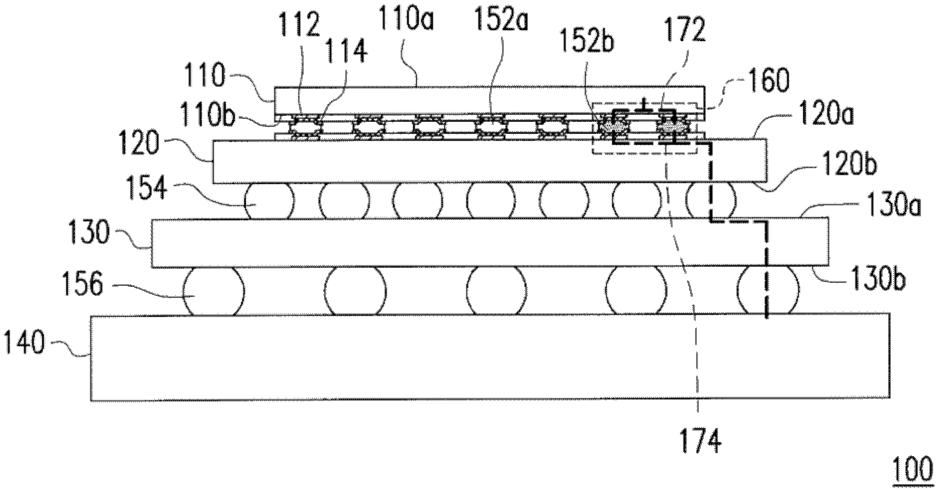
[0017] Reference figure 1 , Which illustrates a semiconductor package structure 100 according to an embodiment of the present invention. The semiconductor package structure 100 is formed by stacking semiconductor elements 110-140.

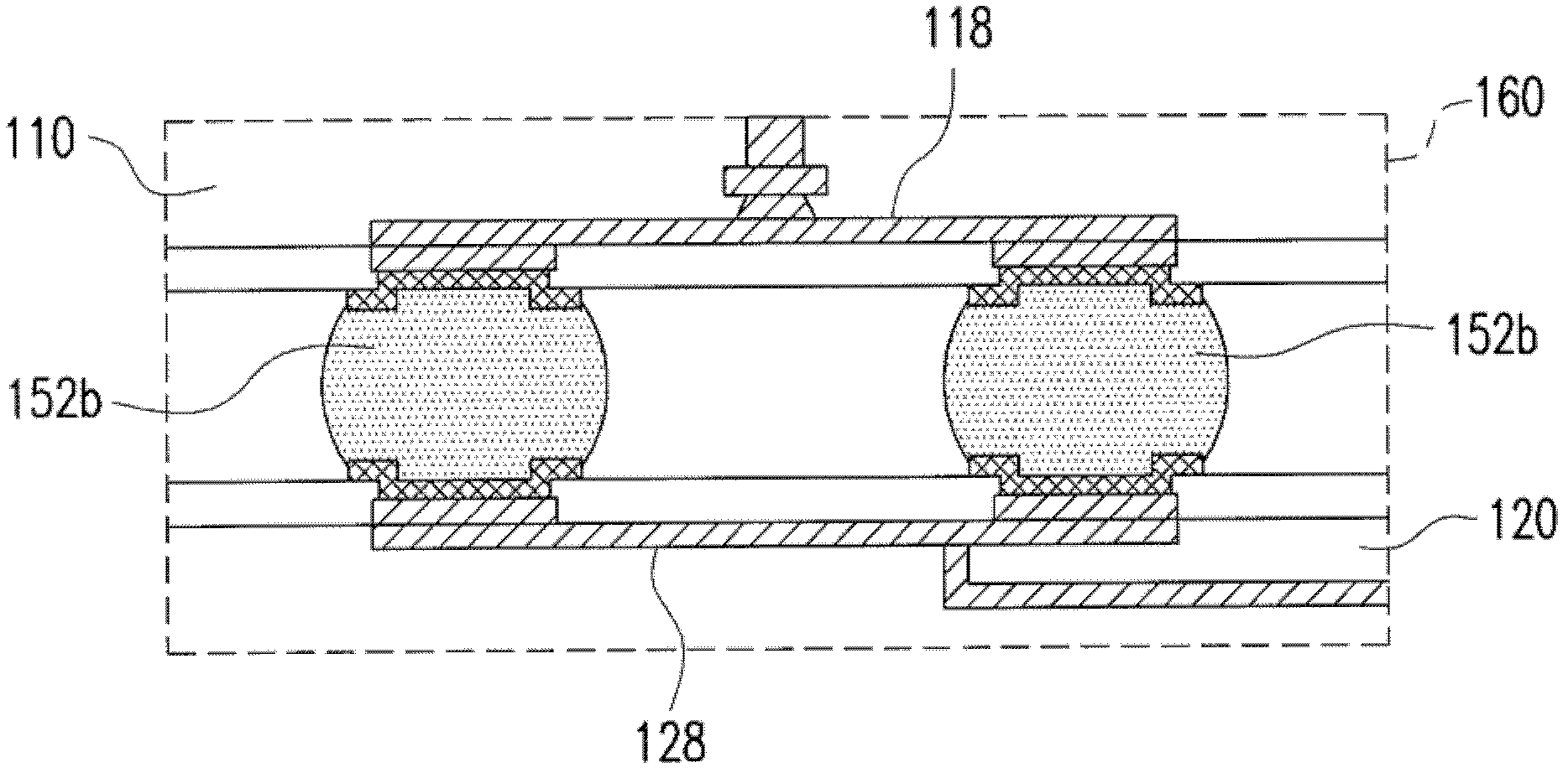
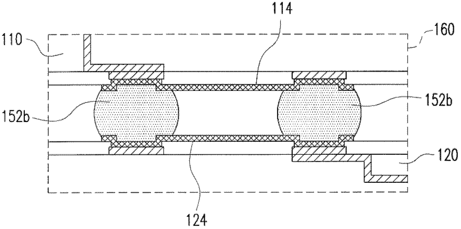
[0018] The semiconductor device 110, in this embodiment, is, for example, a chip, and has an upper surface 110a and a lower surface 110b. The lower surface 110b has a plurality of bonding pads 112, and a plurality of bottom metal layers 114 are disposed on the bonding pads 112. The semiconductor device 110 can be bonded to the semiconductor device 120 through the first bumps 152 a and the second bumps 152 b disposed on the underlying metal layer 114. The first bump 152a is disposed in the middle area of ​​the lower surface 110b of the semiconductor device 110, the second bump 152b is disposed in the corner area of ​​the lower surface 110b of the semiconductor device 110, and the second bump 152b surrounds the first Bumps 152, and the second bump 152b...


PUM


Abstract

The invention discloses a semiconductor packaging structure with multiple convex block structures. The semiconductor packaging structure is formed by stacking multiple semiconductor elements, wherein the corners of the connection surface of two semiconductor elements are provided with multiple convex block structures composed of multiple convex blocks which are conducted mutually; and the multiple convex block structures are used for increasing the extension paths of the cracks on the connection surface of the elements. Thus, when partial convex blocks in the multiple convex block structures lose effectiveness caused by stress failure, other convex blocks in the multiple convex block structures can still maintain normal functions, therefore, the electric connection path between the elements can be prevented from being damaged by stress and losing effectiveness, and further the reliability of the packaging structure is ensured.

Description

Technical field [0001] The invention relates to a semiconductor package structure, and more particularly to a multi-bump structure of a stacked package. Background technique [0002] In the era of the information society, electronic products have become one of the indispensable necessities of life, and a dazzling array of electronic products are flooding the market. With the advancement of electronic technology, many electronic products with strong functionality, fast computing speed and large memory capacity have been developed, but instead of increasing in size, they have moved towards the trend of being lighter, thinner, shorter, and smaller. In order to achieve the purpose of reducing the size and weight, as far as the circuit design is concerned, the concept of integration is integrated. In this way, many functions can be achieved with only one chip, and the integrated circuit with nanometer-level line width can be produced in the chip. The chip integrates many functions, a...

Claims


Application Information

Patent Timeline
Patent Type & Authority Applications(China)
IPC IPC(8): H01L25/065H01L23/535
CPCH01L2224/05569H01L24/05H01L2224/02381H01L2224/0401H01L2224/05558H01L2224/16145H01L2224/16227H01L2224/1703H01L2224/17181H01L2924/15311H01L2224/1411H01L2224/05572H01L2924/14H01L2224/14H01L2224/17107H01L24/17H01L2924/00H01L2924/00012
Inventor 黄东鸿
Owner ADVANCED SEMICON ENG INC
Why Eureka
Try Eureka