
Transmission electron microscope specimen preparation method and transmission electron microscope specimen

A technology for transmission electron microscope samples and areas of concern, applied in the preparation of test samples, etc., can solve problems such as the inability to clearly and accurately characterize metal silicides, and achieve the effect of eliminating ghosting

Inactive Publication Date: 2012-03-14
SEMICONDUCTOR MANUFACTURING INTERNATIONAL (BEIJING) CORP +1
View PDF3 Cites 22 Cited by
  • Summary
  • Abstract
  • Description
  • Claims
  • Application Information

AI Technical Summary

Problems solved by technology

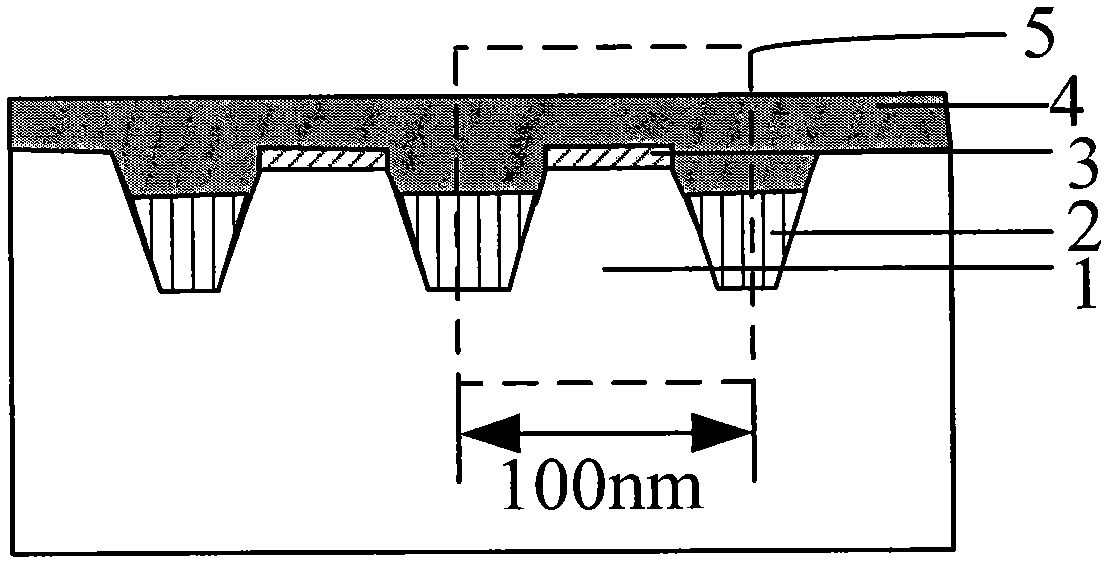
That is to say, in the transmission electron microscope image, the contrast of metal silicide 3 and platinum 4 is included at the same time. Since the contrast of the two in the transmission electron microscope image is very similar, the ghost image formed makes it impossible to clearly and accurately characterize the metal silicide object 3

Method used


Image

  • Transmission electron microscope specimen preparation method and transmission electron microscope specimen
  • Transmission electron microscope specimen preparation method and transmission electron microscope specimen
  • Transmission electron microscope specimen preparation method and transmission electron microscope specimen

Examples


Embodiment 1

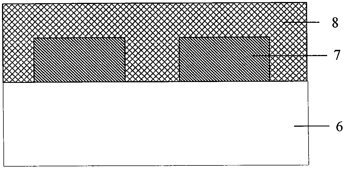
[0042] figure 2 It is a schematic cross-sectional view of a transmission electron microscope sample prepared by an embodiment of the present invention; figure 2 As shown, in this example, the TEM sample includes a region of interest 7, the size of the TEM sample in the lateral direction is less than 100 nm, and the position of the region of interest 7 in the longitudinal direction is higher than that of the surrounding structure 6 of the region of interest , a layer of amorphous thin film 8 is deposited on the attention area, and the amorphous thin film 8 fills up the part of the surrounding structure 6 lower than the attention area 7 and covers the attention area 7. A layer of platinum or tungsten film (not shown) is also deposited on the amorphous film 8, and the contrast difference between the amorphous film 8 and the region of interest 7 in the transmission electron microscope image is greater than that of the region of interest 7 and platinum. Or the contrast differenc...

Embodiment 2

[0047] When the region of interest 7 is a crystal thin film, the transmission electron microscope sample used in the present invention and its preparation method are described in detail.

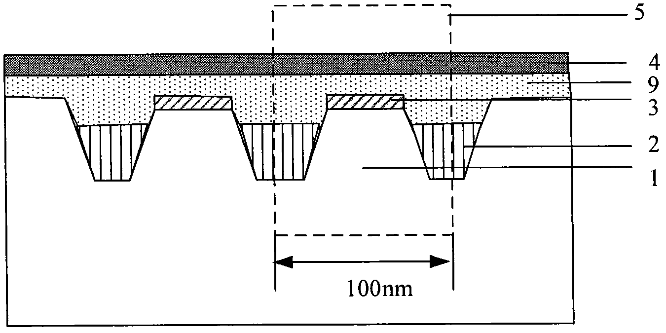
[0048] For an example of one of these crystalline thin films, the metal suicide, see image 3 , which is a structure to be prepared as a transmission electron microscope sample 5, and an active region 1, a shallow trench isolation region 2, and a metal silicide layer 3 on the active region 1 are formed on the substrate. The size of the metal silicide layer 3 in the lateral direction is less than 100 nm, and the position of the metal silicide layer 3 in the longitudinal direction is higher than that of the surrounding shallow trench isolation region 2 . The lateral thickness of the active region 1 is less than 70nm, and is higher than the shallow trench isolation region 2 around it. The active region 1 may be a polysilicon gate or source and drain.

[0049] The method for characterizing the m...

Embodiment 3

[0055] see Figure 4 , the present invention provides a structure to be prepared as a sample 5 for transmission electron microscopy, including polysilicon 11 , metal silicide 10 and shallow trench isolation region 2 . The region of interest is the metal silicide 10 on the polysilicon 11 , the size of which is less than 200 nm in the lateral direction, and the position of the metal silicide 10 in the longitudinal direction is higher than the shallow trench isolation region 2 of the surrounding structure.

[0056] The method for preparing a transmission electron microscope sample by using the above-mentioned structure to be prepared comprises the following steps:

[0057] (1), depositing an amorphous film 13 on the metal silicide 10,

[0058] (2), intercepting the transmission electron microscope sample, the transmission electron microscope sample includes a part of metal silicide 10, polysilicon 11, and amorphous film 13 in its lateral direction, and the size of the transmissi...


PUM

PropertyMeasurementUnit
thicknessaaaaaaaaaa
sizeaaaaaaaaaa
sizeaaaaaaaaaa

Abstract

The invention relates to a transmission electron microscope specimen, which comprises a substrate on which an interest region is arranged on. A dielectric layer and a metal layer are sequentially formed on the substrate and the interest region. The difference between the contrast of the dielectric layer and the contrast of the interest region is larger than a preset value. The preparation method of the transmission electron microscope specimen comprises the steps of: providing the substrate and forming the interest region on the substrate; forming the dielectric layer on the interest region and the substrate; forming the metal layer on the dielectric layer, wherein the difference between the contrast of the dielectric layer and the contrast of the interest region is larger than the preset value; and sectioning the transmission electron microscope specimen, wherein the transmission electron microscope specimen comprises the interest region, the dielectric layer and the metal layer. The preparation method of the transmission electron microscope specimen is simple and feasible and clearer and more accurate transmission electron images can be obtained by using the transmission electron microscope specimen.

Description

technical field [0001] The invention relates to the technical field of semiconductors, in particular to a method for preparing a transmission electron microscope sample and a transmission electron microscope sample. Background technique [0002] Transmission Electron Microscopy (TEM) is a very important tool and means for observing microstructure in the IC industry. Many critical dimensions of online detection need to be compared with the measured values ​​of transmission electron microscopy, which is also an important way to solve many problems of online detection. Usually, technicians analyze each area of ​​interest by observing the contrast of the transmission electron microscope image. The contrast is the difference between the light and dark of the image when analyzing the TEM image. [0003] With the development of advanced processes in the semiconductor industry, critical dimensions are getting smaller and smaller. When the process reaches 65nm, the width of CD (crit...

Claims


Application Information

Patent Timeline
Patent Type & Authority Applications(China)
IPC IPC(8): G01N1/28
Inventor 庞凌华段淑卿陈玉华
Owner SEMICONDUCTOR MANUFACTURING INTERNATIONAL (BEIJING) CORP
Learn More