

Manufacturing method for trench-type power semiconductor
A technology of power semiconductors and manufacturing methods, applied in the direction of semiconductor devices, etc., can solve the problems of increasing the importance of switching losses and achieve the effect of reducing switching losses
- Summary
- Abstract
- Description
- Claims
- Application Information
AI Technical Summary
Problems solved by technology
Method used
Image

Examples
Embodiment Construction
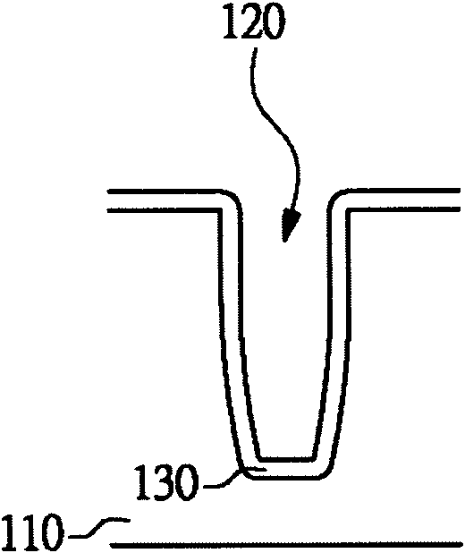
[0027] Figure 1A to Figure 1G A first embodiment of the method for manufacturing a trench power semiconductor according to the present invention is shown. First, if Figure 1A As shown, a substrate 110 is provided. The substrate 110 is doped with the first conductivity type and can be used as a drain region of the power semiconductor structure. In one embodiment, the substrate 110 may be composed of a heavily doped substrate and a lightly doped epitaxial layer covering it. Subsequently, a gate trench 120 is formed in the substrate 110 . Next, a dielectric layer 130 is formed to cover the inner surface of the gate trench 120 . The dielectric layer 130 can be made of silicon oxide or silicon nitride.
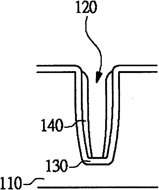
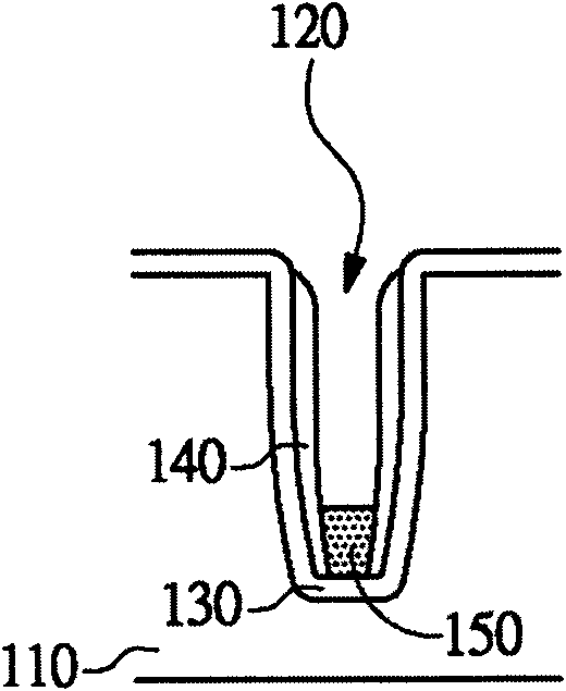
[0028] Subsequently, if Figure 1B As shown, a spacer 140 is formed in the gate trench 120 . The spacer 140 covers the dielectric layer 130 at the sidewall of the gate trench 120 and defines a space at the bottom of the gate trench 120 to expose the dielectric layer 130 at ...
PUM
 Abstract
Description
Claims
Application Information