Method for manufacturing semiconductor device

A manufacturing method and semiconductor technology, which can be used in semiconductor/solid-state device manufacturing, electrical components, circuits, etc., and can solve problems such as gate structure damage

Inactive Publication Date: 2012-03-14
SEMICON MFG INT (SHANGHAI) CORP +1
View PDF5 Cites 9 Cited by
  • Summary
  • Abstract
  • Description
  • Claims
  • Application Information

AI Technical Summary

Problems solved by technology

[0040] However, in the above step 115, since the thickness of the contact hole etch stop layer 1013 is relatively thin, if the dielectric layer 1014 and the contact hole etch stop layer 1013 have a relatively low etching selectivity ratio, then in step 116, when the When the dielectric layer 1014 is etched, it is easy to etch directly to the etch stop layer 1013 of the contact hole and continue to etch below the etch stop layer 1013, thereby causing damage to the gate structure below the contact hole 1015. It can be seen that, In order to avoid damage to the semiconductor device, under the premise that the thickness of the contact hole etch stop layer 1013 is relatively thin, the dielectric layer 1014 and the contact hole etch stop layer 1013 are required to have a high etching selectivity ratio, but the prior art still has no corresponding solution

Method used


Image

  • Method for manufacturing semiconductor device
  • Method for manufacturing semiconductor device
  • Method for manufacturing semiconductor device

Examples


Embodiment Construction

[0061] In order to make the object, technical solution and advantages of the present invention clearer, the solutions of the present invention will be further described in detail below with reference to the accompanying drawings and examples.
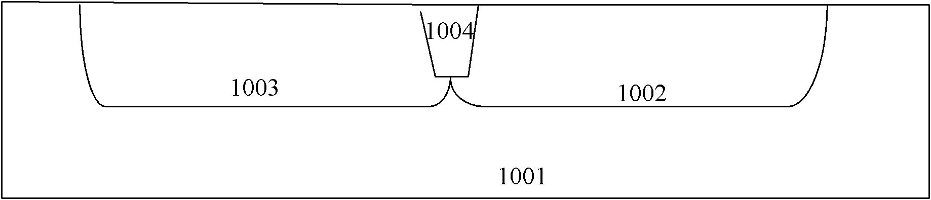
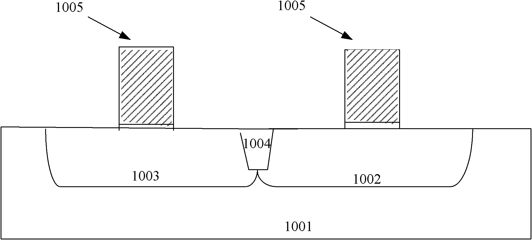
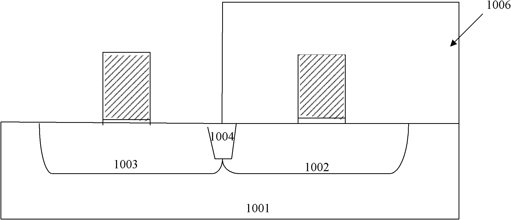
[0062] The core idea of ​​the present invention is: compared with Boron Doped Amorphous Carbon, Fluorin Doped Amorphous Carbon, Chlorine Doped Amorphous Carbon or amorphous Carbon (Amorphous Carbon) has a high etching selectivity ratio, and boron-doped amorphous carbon, fluorine-doped amorphous carbon, chlorine-doped amorphous carbon or amorphous carbon can be used as the main component of the contact hole etching stop layer, so that When the dielectric layer is etched, the damage to the etch stop layer of the contact hole is relatively small, and etching below the etch stop layer of the contact hole is avoided, thereby avoiding damage to the semiconductor device. Further, boron-doped amorphous carbon, fluorine-doped amorphous carbon, c...


PUM

PropertyMeasurementUnit
thicknessaaaaaaaaaa
thicknessaaaaaaaaaa
thicknessaaaaaaaaaa

Abstract

The invention discloses a method for manufacturing a semiconductor device. The method comprises the following steps of: firstly, forming a contact hole etching stop layer which is prepared from boron-doped amorphous carbon, fluorine-doped amorphous carbon, chlorine-doped amorphous carbon or amorphous carbon; secondly, depositing a medium layer on the contact hole etching stop layer, and etching the medium layer and stopping etching on the upper surface of the contact hole etching stop layer to form a groove; and finally, incinerating the contact hole etching stop layer in the groove to form a contact hole. By the method, the damage to the semiconductor device in the process of etching the contact hole can be avoided.

Description

technical field [0001] The invention relates to semiconductor technology, in particular to a manufacturing method of a semiconductor device. Background technique [0002] Figure 1 to Figure 17 It is a process cross-sectional schematic diagram of a manufacturing method of a semiconductor device in the prior art, and the method mainly includes: [0003] Step 101, see figure 1 A semiconductor substrate 1001 is provided, and an N well 1002 , a P well 1003 and a shallow trench isolation region (STI) 1004 are formed on the semiconductor substrate 1001 . [0004] First, the active regions of the N-type metal oxide semiconductor (NMOS) tube and the P-type metal oxide semiconductor (PMOS) tube are defined by using a double well process, thereby obtaining the N well 1002 and the P well 1003, and then, through photolithography and An STI 1004 is formed on the semiconductor substrate 1001 through etching and other processes, and the STI 1004 is used to electrically insulate the acti...

Claims


Application Information

Patent Timeline
Patent Type & Authority Applications(China)
IPC IPC(8): H01L21/8238H01L21/768
Inventor 孙武张海洋周俊卿
Owner SEMICON MFG INT (SHANGHAI) CORP
Why Eureka
Try Eureka