Surface plasmon resonance device

a surface plasmon and plasmon technology, applied in the direction of instruments, optical elements, optics, etc., can solve the problems of inability to measure the dielectric constant by the above-mentioned method, the inability to coupling the electromagnetic wave propagating in the transparent medium with the surface plasmon at the metal-dielectric sample interface, and the inability to achieve the above-mentioned method

Inactive Publication Date: 2005-09-15
SONY CORP
View PDF11 Cites 62 Cited by
  • Summary
  • Abstract
  • Description
  • Claims
  • Application Information

AI Technical Summary

Benefits of technology

[0018] In the present invention, even when a dielectric sample has a higher dielectric constant than that of the transparent medium layer, an electromagnetic wave propagating in the transparent medium layer is strongly coupled with surface plasmons at the interface between the conductive layer and the dielectric sample, thereby permitting measurement of the higher dielectric constant of the dielectric sample than that of the transparent medium layer.

Problems solved by technology

However, when an interface between a dielectric material and a conductive material such as a metal or the like is planar, an electromagnetic wave propagating in the dielectric material cannot be coupled with the plasmons in the conductive material.
However, for a sample having a higher dielectric constant than that of a transparent medium, the dielectric constant cannot be measured by the above-mentioned method.
Thus, an electromagnetic wave propagating in the transparent medium cannot be coupled with surface plasmons at the metal-dielectric sample interface.
Consequently, there is the problem that the dielectric constant of the sample cannot be measured with light incident on the transparent medium layer.

Method used


Image

  • Surface plasmon resonance device
  • Surface plasmon resonance device
  • Surface plasmon resonance device

Examples


example 1

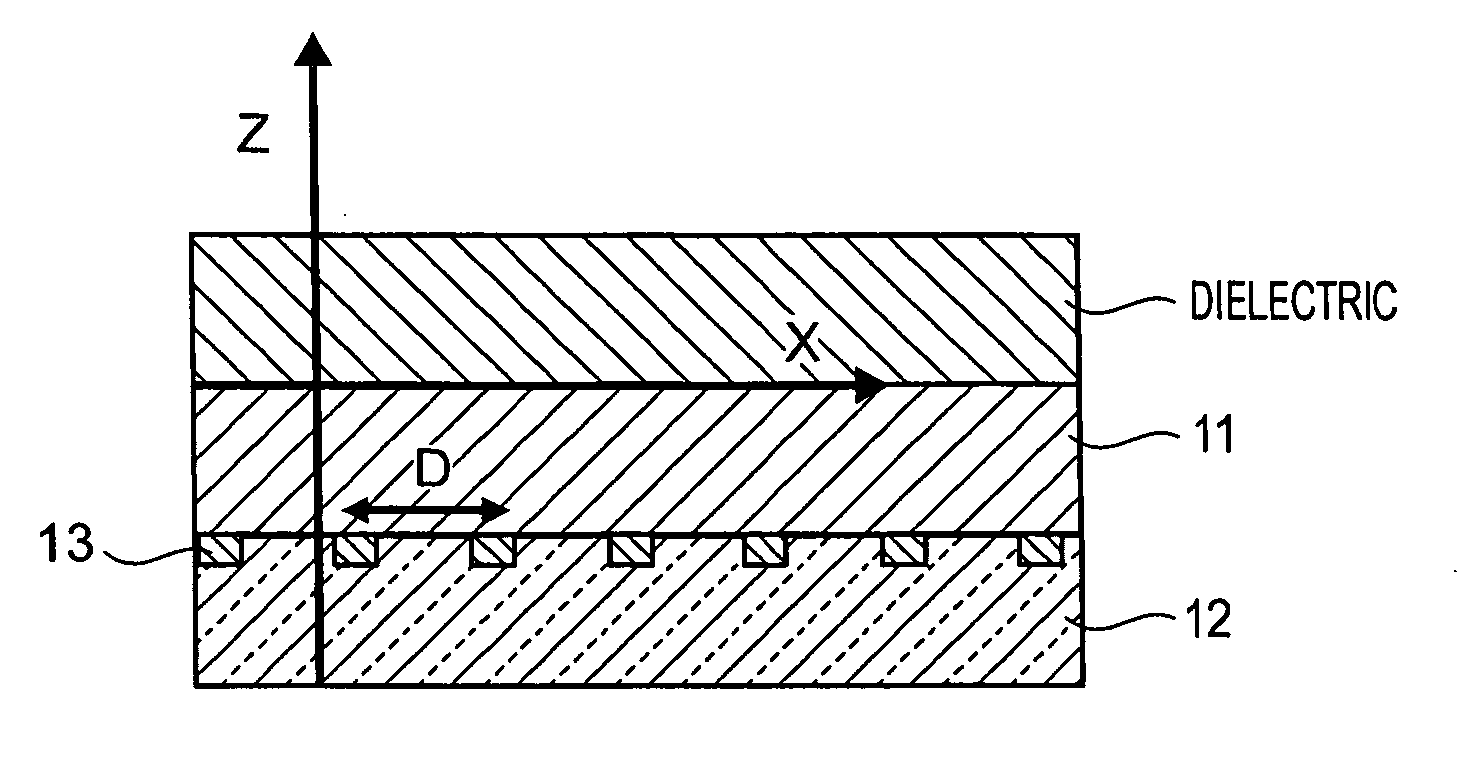
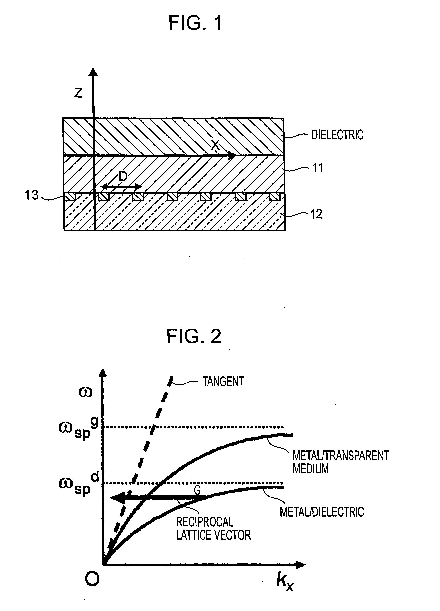
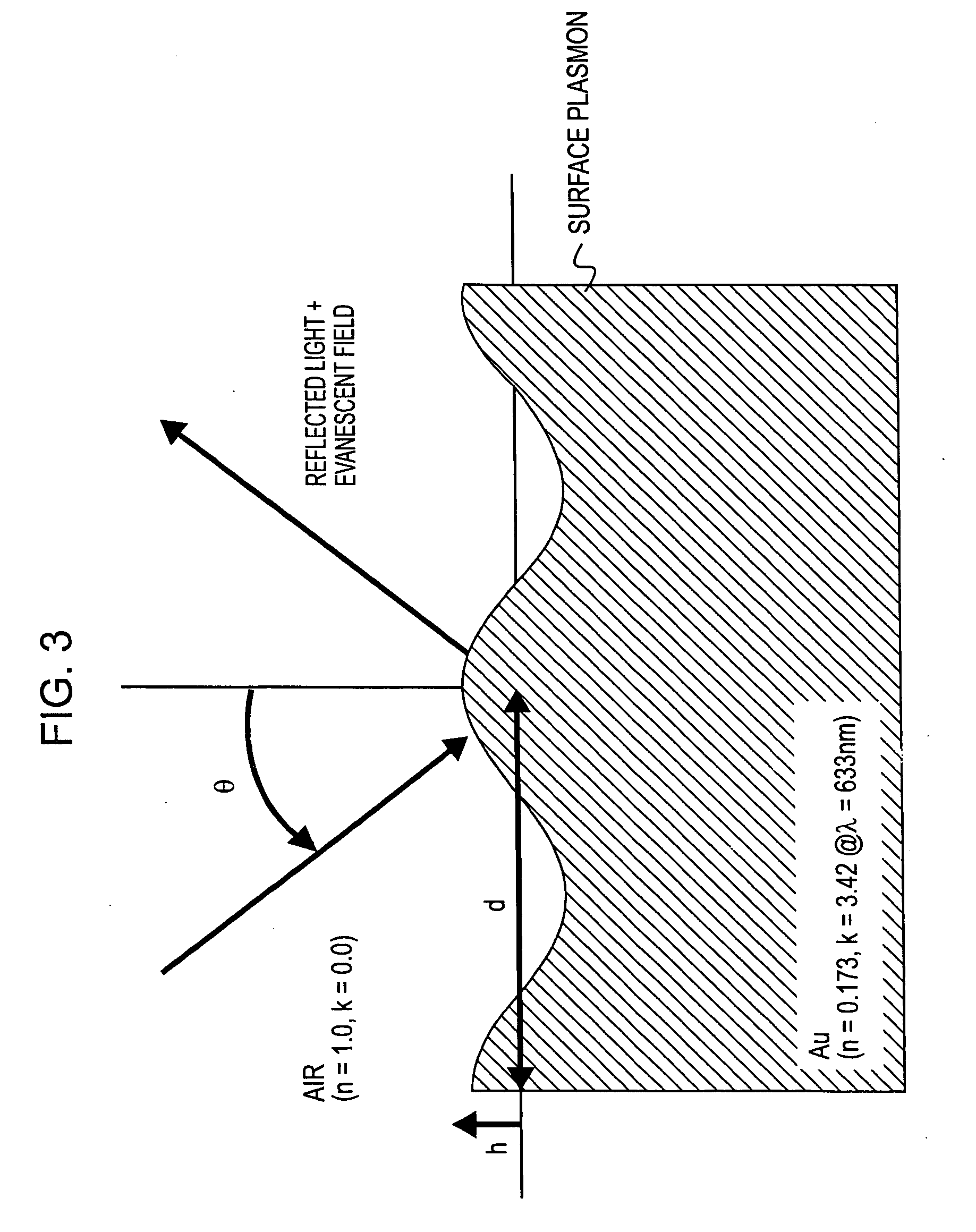
[0050]FIG. 10 shows a surface plasmon resonance device of Example 1. As shown in FIG. 10, the surface plasmon resonance device uses a glass substrate as a transparent medium layer 12, and micro structures 14 each comprising a gold fine particle or a micro cylinder are periodically buried in the transparent medium layer 15 comprising, for example, glass or a material having the same dielectric constant as that of glass, thereby forming a periodic structure 13. The micro structures 14 can be formed by, for example, micro patterning or a template using phase separation (for example, a nano-template formed by spreading a polystyrene / polyisoprene block copolymer on a substrate to form a sea island-like micro phase-separation structure, and then removing the polyisoprene by ozone oxidative decomposition to form nano-pores). Furthermore, a gold thin film is formed as a metal layer 11 on the transparent medium layer 15. The gold thin film can easily be formed by vapor deposition, sputtering...

example 2

[0052]FIG. 11 shows a surface plasmon resonance device of Example 2. As shown in FIG. 11, the surface plasmon resonance device comprises a glass substrate used as a transparent medium layer 12, and a gold thin film 16 formed thereon. Furthermore, pores 17 are periodically formed in the gold thin film 16, the pores 17 being filled with glass or a transparent medium layer 18 having the same dielectric constant as that of glass to form a periodic structure 13. The pores 17 can be easily formed by irradiating the gold thin film 16 with an electron beam or the like. Furthermore, a gold thin film is formed as a metal layer 11 on the gold thin film 16. The gold thin film can be easily formed by vapor deposition, sputtering, or the like.

[0053] The material constituting the transparent medium layer 12 is not limited to glass, and any one of other materials transparent in the visible region, for example, plastics and the like, may be used. The material constituting the micro structures 14 is...


PUM

PropertyMeasurementUnit
thicknessaaaaaaaaaa
plasma frequencyaaaaaaaaaa
wavelengthaaaaaaaaaa

Abstract

A surface plasmon resonance device of the present invention includes a transparent medium layer and a conductive layer, a periodic structure being present at the interface therebetween. Assuming that the wavelength of visible light incident on the conductive layer through the transparent medium layer is λ (nm), the periodicity of the periodic structure is (λ / 633)×100 nm to (λ / 633)×500 nm, and the amplitude of the periodic structure is (λ / 633)×5 nm to (λ / 633)×20 nm. For example, when λ=633 nm, the periodicity of the periodic structure is 100 nm to 500 nm, and the amplitude is 5 nm to 20 nm.

Description

BACKGROUND OF THE INVENTION [0001] 1. Field of the Invention [0002] The present invention relates to a surface plasmon resonance device, and particularly to a surface plasmon resonance device suitably used for measuring the dielectric constants of various samples. [0003] 2. Description of the Related Art [0004] A conventional known method for measuring the dielectric constant of a surface of a sample is a surface plasmon resonance method (for example, Japanese Unexamined Patent Application Publication No. 11-271215). Among modes of plasmons referring to collective resonance of free electrons present in a conductive material such as a metal or the like, the conventional method uses a surface plasmon mode in which plasmons are localized at a surface of the conductive material. The principle of measurement is as follows: Surface plasmons are coupled with an electromagnetic wave in a dielectric material at an interface between the dielectric material and a conductive material such as a ...

Claims


Application Information

Patent Timeline
Patent Type & Authority Applications(United States)
IPC IPC(8): G02B6/00G01N21/27
CPCB82Y20/00G02B6/1226G01N21/553
Inventor MATSUMURA, HAJIME
Owner SONY CORP
Why Eureka
Try Eureka