Method of improving consistence and stability of LDMOS (Laterally Diffused Metal Oxide Semiconductor) performance

A consistent and stable technology, applied in electrical components, semiconductor/solid-state device manufacturing, circuits, etc., can solve problems affecting device performance consistency, etc., to improve consistency and stability, improve uniformity, and reduce width. effect of difference

Inactive Publication Date: 2012-03-21
SHANGHAI HUAHONG GRACE SEMICON MFG CORP
View PDF5 Cites 4 Cited by
  • Summary
  • Abstract
  • Description
  • Claims
  • Application Information

AI Technical Summary

Problems solved by technology

Thereby seriously affecting the consistency of device performance

Method used


Image

  • Method of improving consistence and stability of LDMOS (Laterally Diffused Metal Oxide Semiconductor) performance
  • Method of improving consistence and stability of LDMOS (Laterally Diffused Metal Oxide Semiconductor) performance
  • Method of improving consistence and stability of LDMOS (Laterally Diffused Metal Oxide Semiconductor) performance

Examples


Embodiment Construction

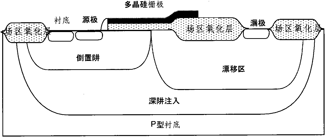
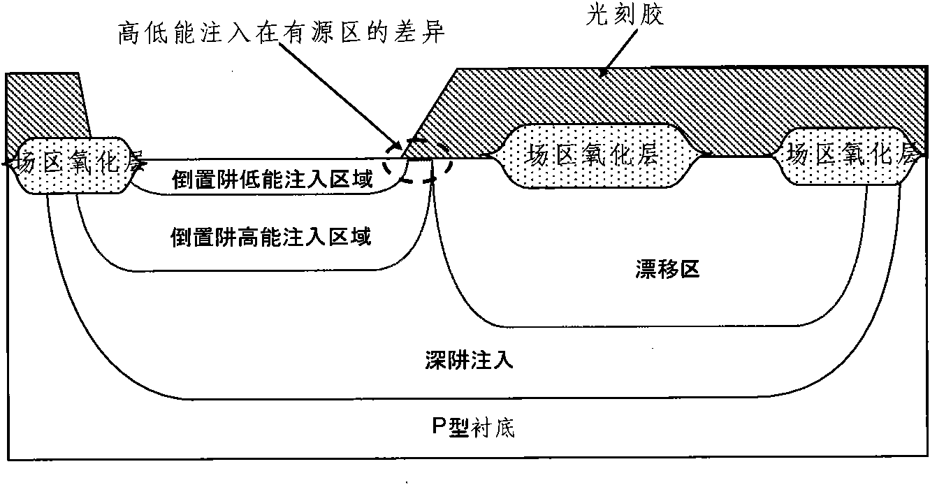
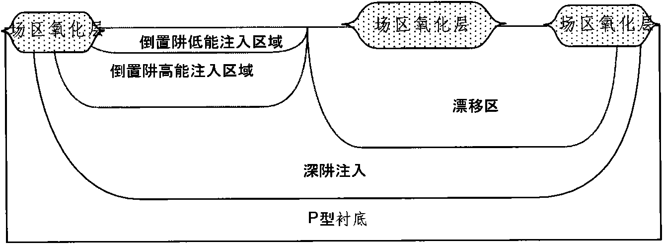
[0035] Such as image 3 As shown, the key of the present invention is to adjust the size of the photolithography window between high-energy and low-energy implantation, narrow the difference in width between high-energy and low-energy implantation, and improve the uniformity of impurity distribution in the LDMOS channel. Therefore, the consistency and stability of the performance of the LDMOS device are improved.

[0036] Such as Figure 4-Figure 7 As shown, a method for improving the consistency and stability of laterally diffused metal oxide semiconductor device performance by using plasma etching to adjust the size of the photolithographic window for protecting between high-energy and low-energy implants according to the present invention includes: :

[0037] Step 1, using photolithography to form an inverted well and inject a photoresist window;

[0038] Step 2, high-energy ion implantation;

[0039] Step 3, using plasma etching to expand the photoresist window;

[00...


PUM


Abstract

The invention discloses a method of improving consistence and stability of LDMOS (Laterally Diffused Metal Oxide Semiconductor) performance; between high energy injection and low energy injection, the size of a photoetching window is adjusted by utilizing plasma etching, and the method comprises the following steps: step one, forming an inverted pit photoresist injection window by utilizing photoetching; step two, injecting high energy ions; step three, expanding the size of the photoetching window by utilizing plasma etching; step four, injecting low energy ions; and step five, removing the photoresist. In the invention, the size of the photoetching window is adjusted between high energy injection and low energy injection, width difference between high energy injection and low energy injection is shortened, and the uniformity of impurity distribution in an LDMOS channel can be improved. Therefore, the consistence and the stability of the LDMOS device can be improved.

Description

technical field [0001] The invention relates to an integrated circuit manufacturing technology, in particular to a manufacturing method of a lateral diffusion metal oxide semiconductor device LDMOS. Background technique [0002] In power and high-voltage integrated circuits, low-voltage inverted well implants are often used as body implants for high-voltage LDMOS (laterally diffused metal-oxide semiconductor devices) (such as figure 1 shown). Inverted well implants generally include high-energy well implants and low-energy turn-on voltage adjustment implants. The thickness of the photoresist used in the injection is greater than 0.5 microns, and the body pattern density of the LDMOS device is relatively low, so the inclination angle of the edge of the photoresist window of the LDMOS is generally large, and the inclination angle of the photoresist will vary with the The difference of the lithography machine and the change of the channel direction of the device. Due to the ...

Claims


Application Information

Patent Timeline
Patent Type & Authority Applications(China)
IPC IPC(8): H01L21/336H01L21/265H01L21/311
Inventor 陈瑜罗啸吴智勇
Owner SHANGHAI HUAHONG GRACE SEMICON MFG CORP
Why Eureka
Try Eureka