Technological method of ONO side wall

A process method and sidewall technology, which is applied in the manufacture of electrical components, circuits, semiconductors/solid-state devices, etc., to achieve the effect of reducing the difference in sidewall width

Active Publication Date: 2021-03-02
HUA HONG SEMICON WUXI LTD
View PDF5 Cites 0 Cited by
  • Summary
  • Abstract
  • Description
  • Claims
  • Application Information

AI Technical Summary

Problems solved by technology

[0008] The technical problem to be solved by the present invention is to provide a process method for ONO sidewalls to reduce the difference in the thickness of sidewalls between polysilicon dense areas and sparse areas.

Method used


Image

  • Technological method of ONO side wall
  • Technological method of ONO side wall
  • Technological method of ONO side wall

Examples


Embodiment Construction

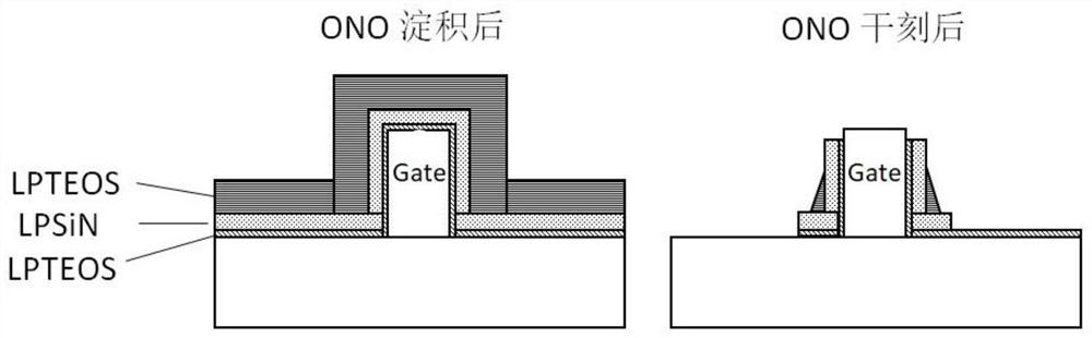
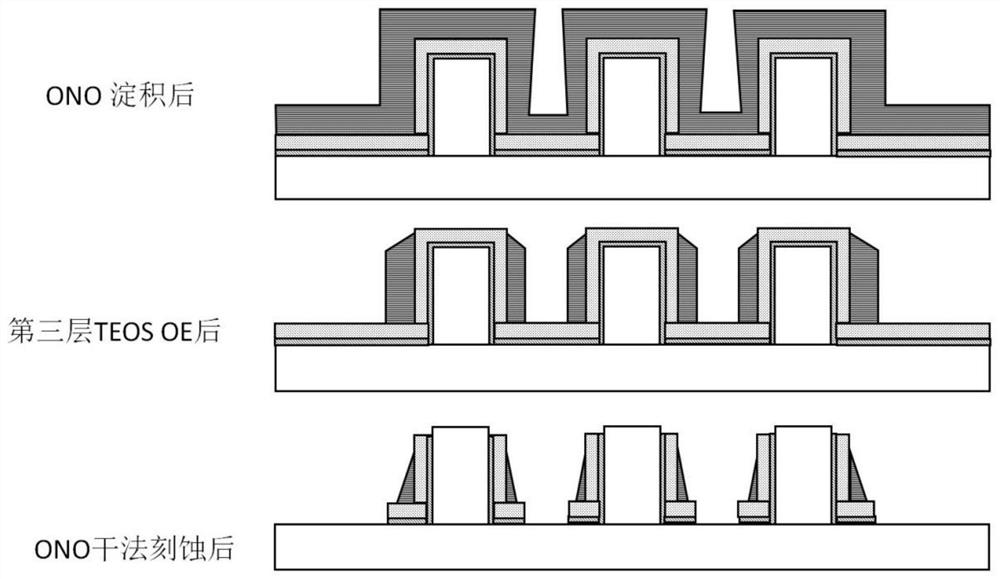
[0020] The present invention is used in the process of using the ONO structure as the side wall in the manufacture of submicron integrated circuits. The process method of the ONO side wall is described as follows in conjunction with the accompanying drawings:

[0021] After the transistors are formed on the wafer, due to the chip layout, the distribution of the transistors is uneven. The polysilicon gates of the transistors and the polysilicon gates formed by connecting the polysilicon gates constitute the dense and sparse areas of the polysilicon gates. First, the first layer, which is the innermost oxide layer, is formed using the traditional process, which is generally formed based on the LPTEOS process, with a deposition thickness of 150Å, and then the second layer, which is the middle layer of silicon nitride, is deposited using the LPCVD process. Formed to a thickness of 300Å. Therefore, depositing the first layer and the middle layer of the ONO sidewall is no different ...


PUM

PropertyMeasurementUnit
thicknessaaaaaaaaaa
thicknessaaaaaaaaaa
thicknessaaaaaaaaaa

Abstract

The invention discloses a technological method of an ONO side wall, and the TOES layer at the minimum silicon gate spacing can be connected into a whole by increasing the TEOS thickness of the outermost layer. And after the etching is started, the TEOS of the sparse region is normally etched. And the TEOS with connected tops needs to be etched in the dense region. After the top TEOS is etched, theTEOS on the side wall of the silicon gate is etched, so that the transverse etching time of the TEOS on the side wall of the polysilicon gate in the sparse region is longer than that of the TEOS in the dense region, the difference that the transverse thickness of the sparse region is greater than that of the dense region is balanced, and the width of the SiN in the middle layer of the side wall is determined by the transverse thickness of the TEOS; and finally, the difference of the thicknesses of the side walls of the dense region and the sparse region is balanced.

Description

technical field [0001] The invention relates to the field of semiconductors, in particular to a process method for ONO sidewalls. Background technique [0002] In the manufacture of submicron integrated circuits, the sidewall process defines the source and drain lightly doped regions, and its width has an important impact on the threshold voltage, leakage current and saturation current of short channel devices. [0003] ONO sidewall is a very widely used sidewall forming process. Such as figure 1 As shown in the left picture in the middle, the gate is in the middle, and the first layer (inner layer) wrapped around the gate is a thin layer of LPTEOS (low-voltage TEOS), about 150Å. The second layer is LPSiN (silicon nitride formed by LPCVD process) with a thickness of about 300Å. The third layer (the outer layer) is thicker LPTEOS, with a thickness ranging from 400 to 1000Å. [0004] After the etching of the ONO sidewall is completed, the lateral width of the "L" type SiN ...

Claims


Application Information

Patent Timeline
Patent Type & Authority Applications(China)
IPC IPC(8): H01L21/308
CPCH01L21/3086H01L21/3083
Inventor 任小兵熊伟陈华伦
Owner HUA HONG SEMICON WUXI LTD
Why Eureka
Try Eureka