Clock generation circuit

A clock generation circuit, a technology for inputting a clock, applied in the direction of electrical pulse generator circuits, electrical components, generating/distributing signals, etc., can solve problems such as PLL loss of synchronization

Inactive Publication Date: 2014-07-30
YAMAHA CORP
View PDF6 Cites 0 Cited by
  • Summary
  • Abstract
  • Description
  • Claims
  • Application Information

AI Technical Summary

Problems solved by technology

If the reference clock CLKREF having a large phase difference with respect to the feedback clock CLKFB is output to the phase comparator 3, a large phase error signal is generated and thus the PLL loses synchronization

Method used


Image

  • Clock generation circuit
  • Clock generation circuit
  • Clock generation circuit

Examples


no. 1 example

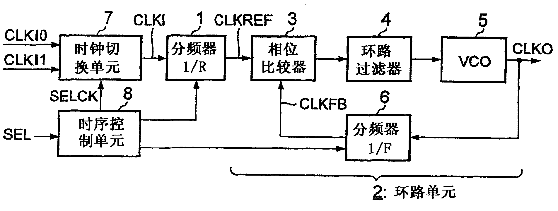
[0034] figure 1 is a block diagram showing the basic configuration of the clock generation circuit according to the first embodiment of the present invention. exist figure 1 , the circuit configuration of the part having frequency divider 1 and loop unit 2 is basically the same as Figure 12 same as shown in .

[0035] The clock generation circuit according to the first embodiment of the present invention is characterized by a clock switching unit 7 and a timing control unit 8 added to a circuit having a frequency divider 1 and a loop unit 2 . The input clocks CLKI0 and CLKI1 having frequencies different from each other are output to the clock switching unit 7 . The clock switching unit 7 selects one of the input clocks CLKI0 and CLKI1 according to the clock selection command SELCK output from the timing control unit 8 and supplies the selected clock to the frequency divider 1 as the input clock CLKI. The timing control unit 8 generates a clock selection command SELCK for...

no. 2 example

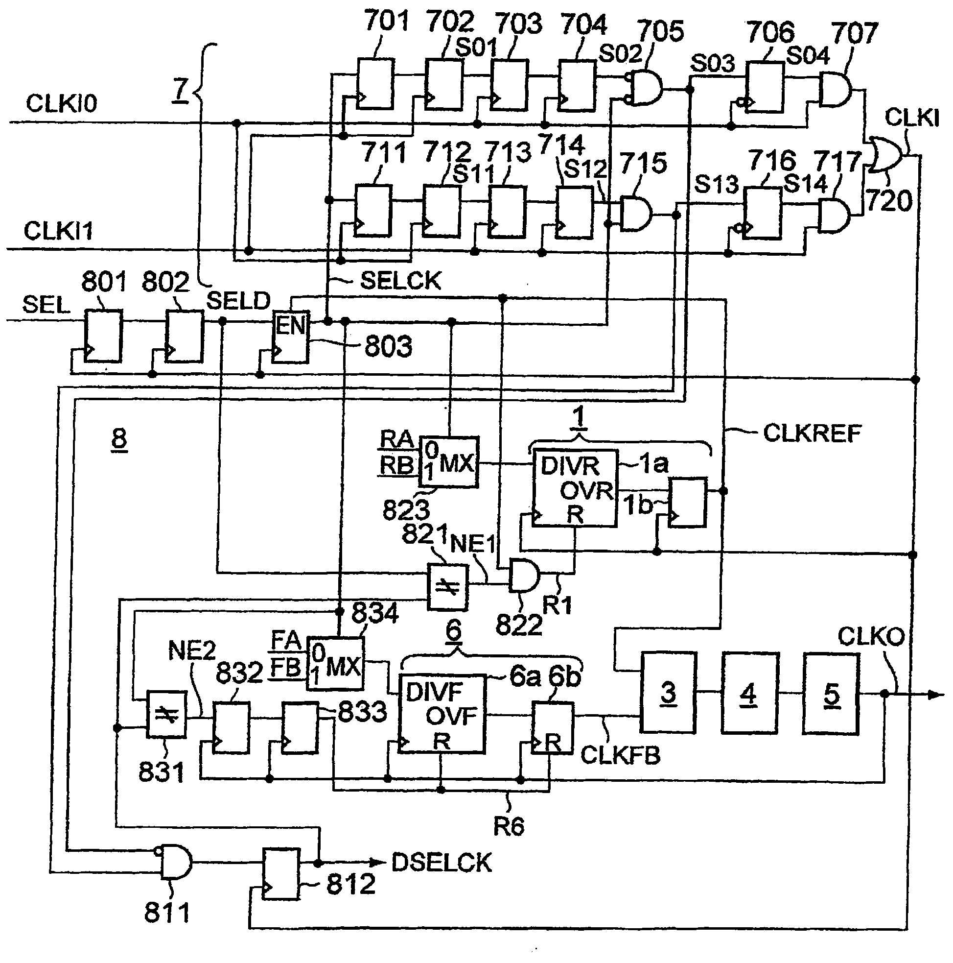
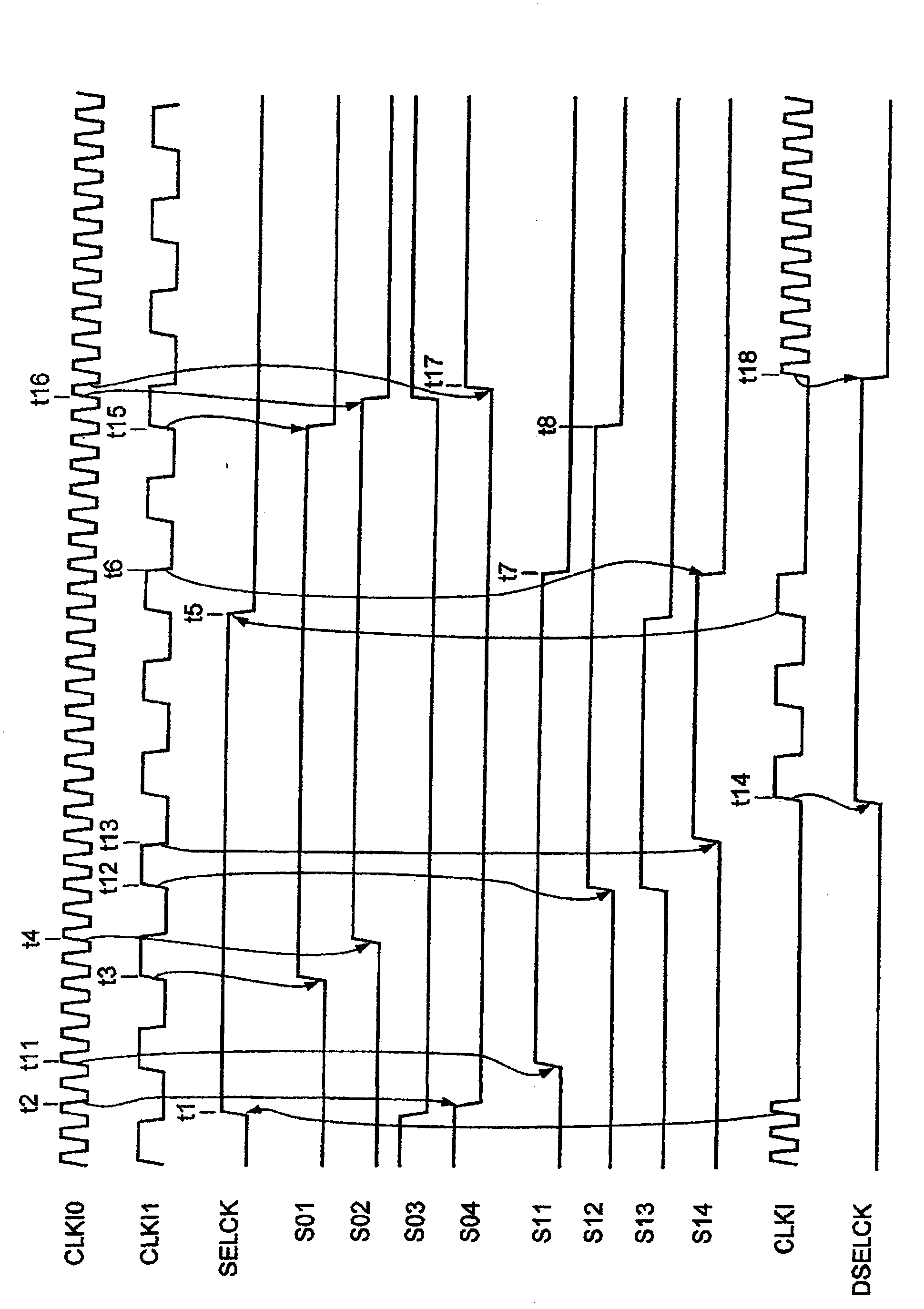
[0077] Figure 8 is a circuit diagram showing the configuration of a clock generating circuit according to a second embodiment of the present invention. Figure 9 is a timing chart showing the outline operation of the clock generation circuit, and Figure 10 is a time chart showing waveforms of respective units according to an embodiment of the present invention. According to the first embodiment of the present invention described above, in the case of switching the clock selection information SEL, the count value CNT1 of the input clock CLKI in the frequency divider 1 becomes "0" thereafter, and when the reference clock CLKREF is output, The clock selection command SELCK is switched to match the clock selection information SEL. According to the second embodiment of the present invention, such as Figure 9 As shown in , for example, in the case where the clock selection information SEL is switched from "0" to "1" in the period in which the frequency divider 1 performs the f...


PUM


Abstract

The invention provides a clock generating circuit. The clock generation circuit includes: a first frequency divider; a loop unit having a second frequency divider and generating an output clock that is phase-synchronous with a reference clock of the first frequency divider and has a frequency that is F times the reference clock a frequency; a clock switching unit that selects one input clock among the plurality of input clocks and supplies the selected input clock to the first frequency divider; and a timing control unit. The timing control unit switches the clock selection command according to the switching of the clock selection information, switches at least one of the setting of the number R of the input clock and the setting of the number F of the output clock, and starts using the first frequency division after switching the setting counting operation of the frequency divider and counting operation using the second frequency divider.

Description

technical field [0001] The present invention relates to a clock generation circuit using a PLL (Phase Locked Loop). Background technique [0002] A PLL is a circuit that generates a phase-locked clock from an input signal, and has been used in various fields. Figure 12 It is a block diagram illustrating the general structure of a PLL. exist Figure 12 Among them, the frequency divider 1 divides the input clock CLKI by a predetermined frequency division ratio 1 / R, and outputs the reference clock CLKREF having a frequency of 1 / R of the input clock CLKI to the phase comparator 3 of the loop unit 2 . The loop unit 2 is a circuit in which a phase comparator 3 , a loop filter 4 , a VCO (Voltage Controlled Oscillator) 5 , and a frequency divider 6 are connected in a loop form. Here, the phase comparator 3 compares the phases of the reference clock CLKREF and the feedback clock CLKFB output from the frequency divider 6, and outputs a phase error signal representing a phase error b...

Claims


Application Information

Patent Timeline
Patent Type & Authority Patents(China)
IPC IPC(8): H03K3/02
CPCG06F1/08H03L7/18
Inventor 浦纯也
Owner YAMAHA CORP
Why Eureka
Try Eureka