D trigger provided with scanning structure and resisting single event upset

An anti-single-event, trigger technology, applied in the direction of electrical pulse generator circuits, pulse generation, electrical components, etc., can solve the problem of low anti-single-event flipping ability.

Active Publication Date: 2013-12-11
NAT UNIV OF DEFENSE TECH
View PDF5 Cites 0 Cited by
  • Summary
  • Abstract
  • Description
  • Claims
  • Application Information

AI Technical Summary

Problems solved by technology

[0008] The technical problem to be solved in the present invention is, aiming at the problem that the anti-single event flip-flop of the scanning structure D flip-flop is not high in anti-single event flip-flop, a kind of anti-single event flip-flop of the scanning structure D flip-flop is proposed, which can be used at a higher Normal operation under single event bombardment of LET values ​​without single event flipping

Method used


Image

  • D trigger provided with scanning structure and resisting single event upset
  • D trigger provided with scanning structure and resisting single event upset
  • D trigger provided with scanning structure and resisting single event upset

Examples


Embodiment Construction

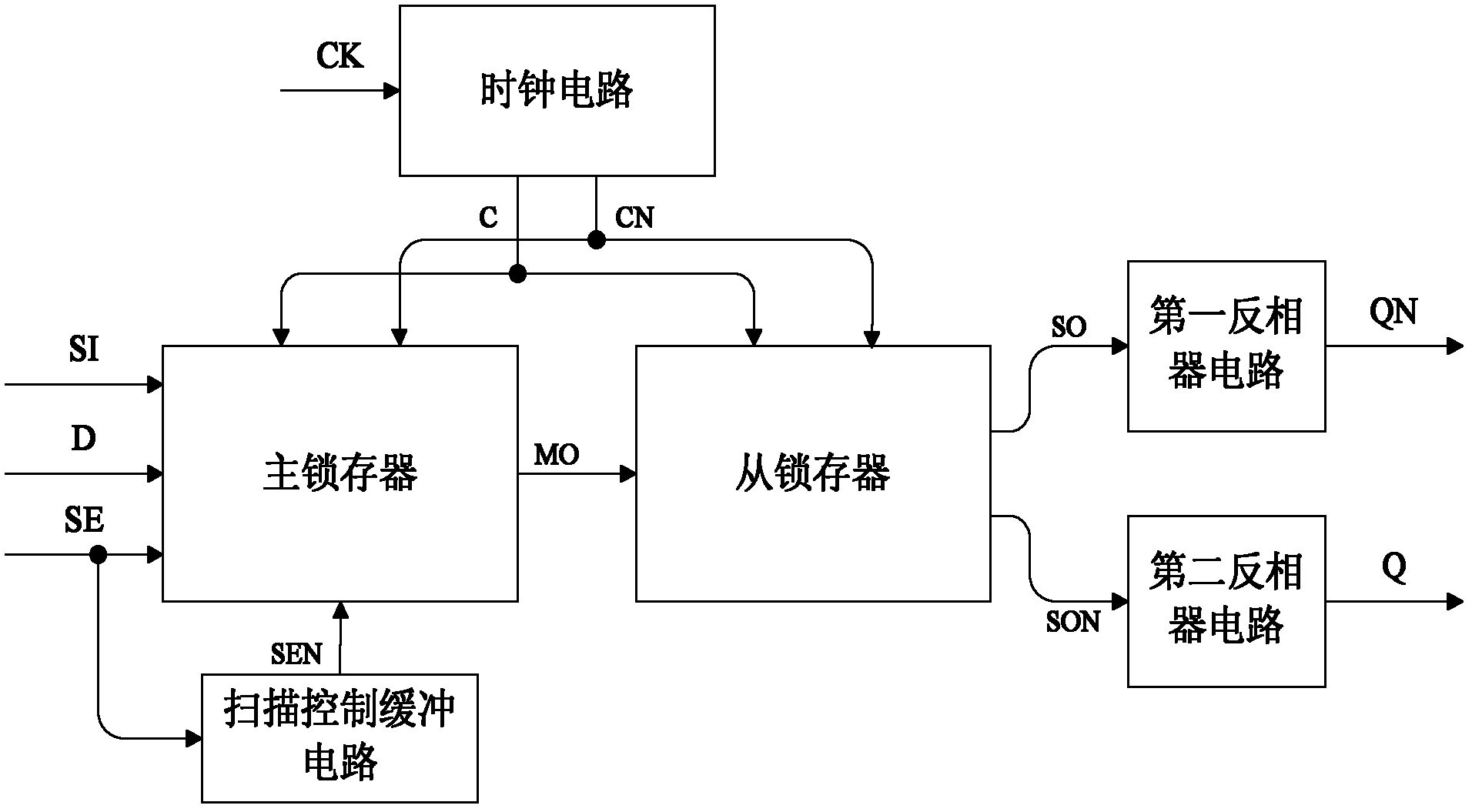
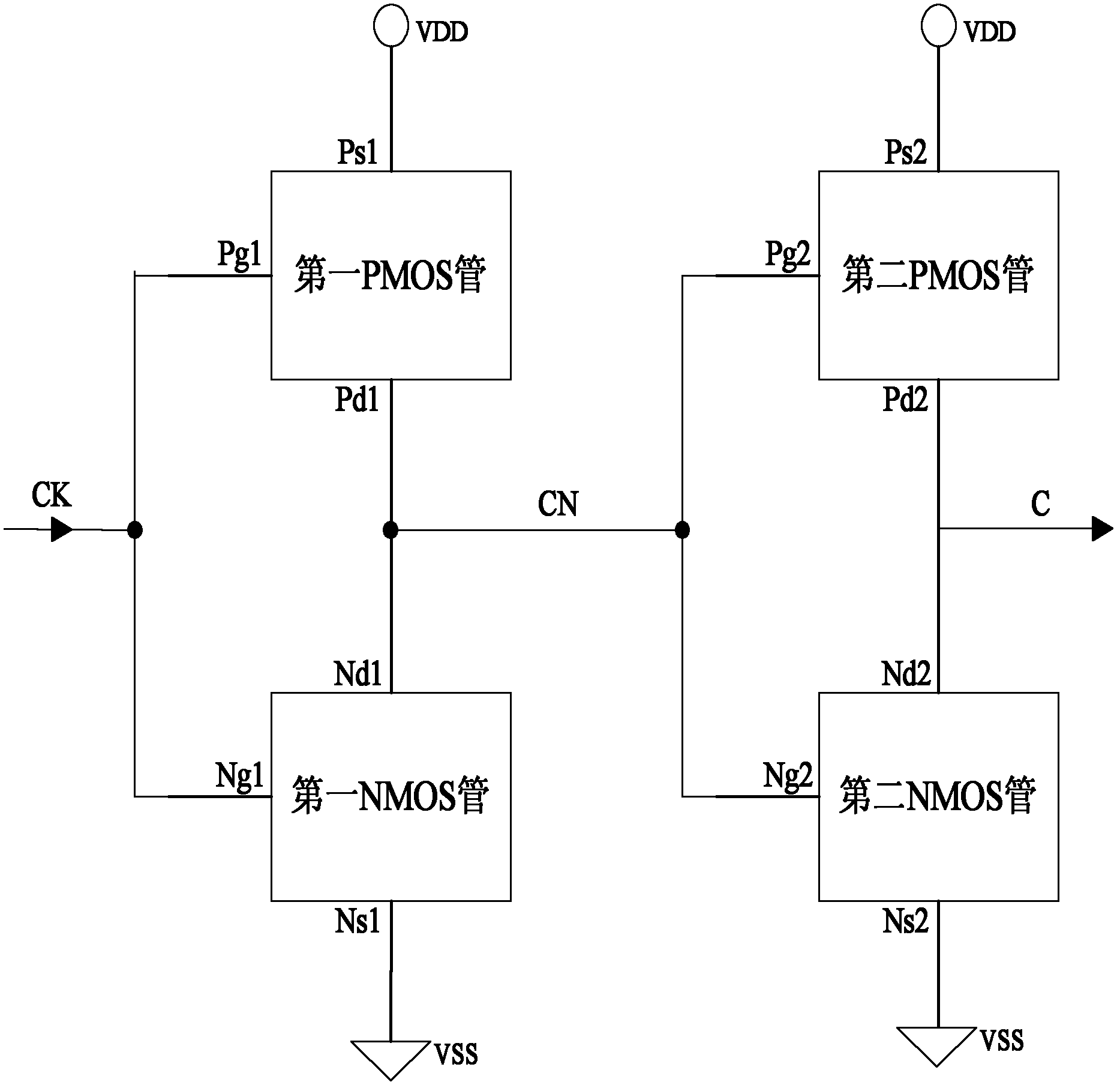
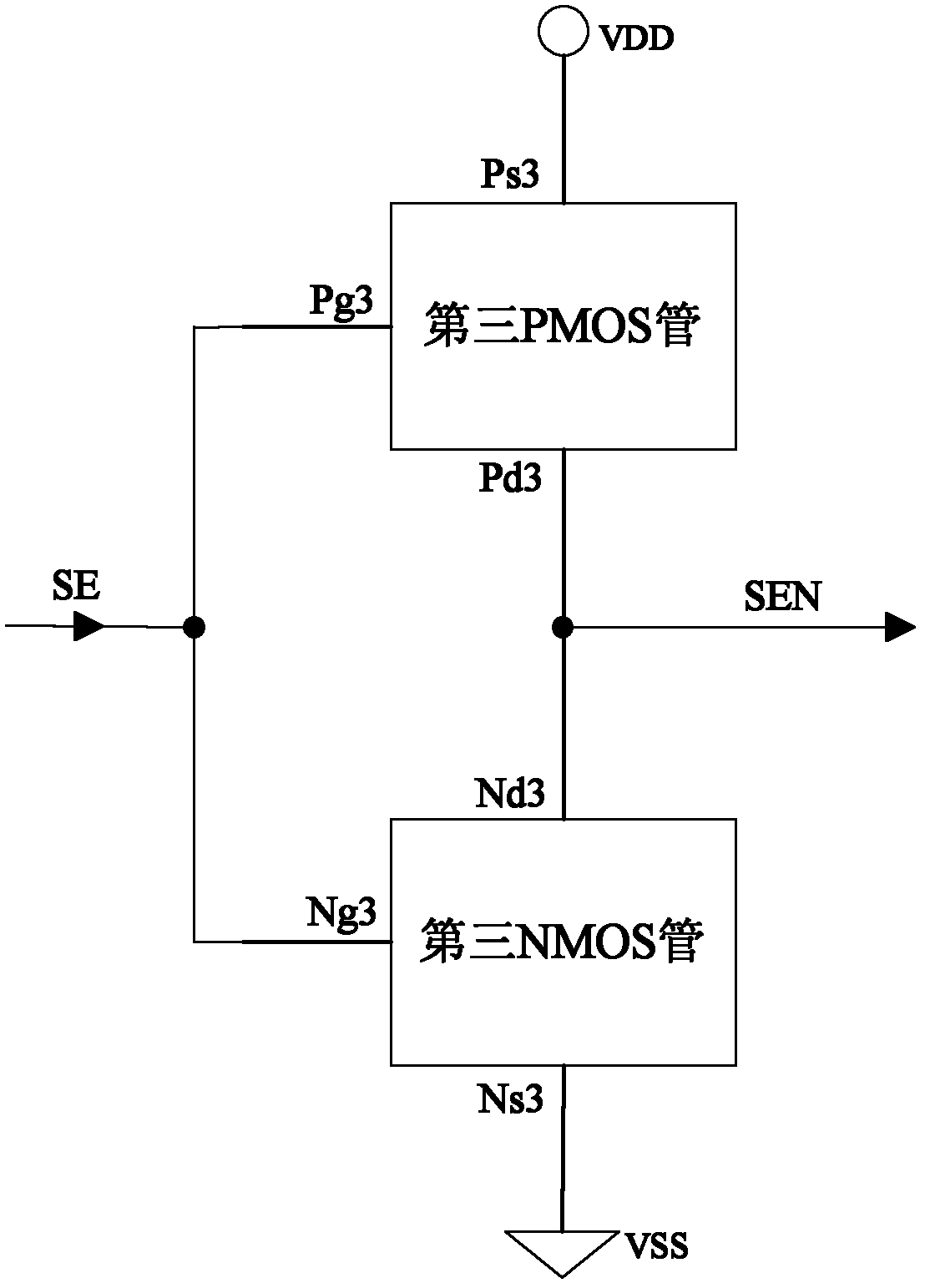
[0031] figure 1 It is a schematic diagram of the logic structure of the anti-single event flip-flop scanning structure D flip-flop of the present invention. The present invention consists of a clock circuit (such as figure 2 shown), scan control buffer circuit (such as image 3 shown), the master latch (as Figure 4 shown), slave latches (as Figure 5 shown), the first inverter circuit (such as Figure 6 shown) and a second inverter circuit (as Figure 7 shown) composition. The present invention has four inputs and two outputs. The four input terminals are CK, which is the clock signal input terminal, D, which is the data signal input terminal, SE, which is the scanning control signal input terminal, and SI, which is the scanning data input terminal; the two output terminals are Q and QN respectively, and Q and QN output one to the opposite data signal. The clock circuit receives CK, and outputs C and CN respectively after buffering CK. The scan control buffer circui...


PUM


Abstract

The invention discloses a D trigger provided with a scanning structure and resisting single event upset, and aims to improve the single event upset resistance of the D trigger provided with the scanning structure. The D trigger comprises a clock circuit, a scanning control buffer circuit, a main latch, a slave latch, a first phase inverter circuit and a second phase inverter circuit, wherein the main latch comprises 16 PMOS (P-channel Metal Oxide Semiconductor) tubes and 16 NMOS (N-Mental-Oxide-Semiconductor) tubes; the slave latch comprises 10 PMOS tubes and 10 NMOS tubes; both the main latch and the slave latch adopt bimodule redundant reinforcement; and in the main latch and the slave latch, C2MOS circuits are improved, that is, a pull-up circuit and a pull-down circuit in redundant relation in each C2MOS circuit are separated. The D trigger has strong single event upset resistance, is suitable for standard cell library for a reinforced integrated circuit resisting single event upset, and is used in the fields of aviation, aerospace, and the like.

Description

technical field [0001] The invention relates to a master-slave D flip-flop with scanning structure, in particular to a scanning structure D flip-flop resistant to single event upset (signal event upset). Background technique [0002] In the universe, there are a large number of high-energy particles (protons, electrons, heavy ions) and charged particles. After the integrated circuit is bombarded by these high-energy particles and charged particles, an electronic pulse will be generated in the integrated circuit, which may cause the original level of the internal node of the integrated circuit to flip. This effect is called single event upset (SEU). The higher the LET (Linear Energy Transfer) value of a single event bombarding an IC, the stronger the resulting electron pulse. Integrated circuits used in aviation and aerospace fields are threatened by single event upsets, which can make integrated circuits work unstable and even cause fatal errors. Therefore, it is particular...

Claims


Application Information

Patent Timeline
Patent Type & Authority Patents(China)
IPC IPC(8): H03K3/013H03K19/003H03K3/02
Inventor 池雅庆孙永节李鹏梁斌杜延康刘必慰陈建军何益百秦军瑞
Owner NAT UNIV OF DEFENSE TECH
Why Eureka
Try Eureka