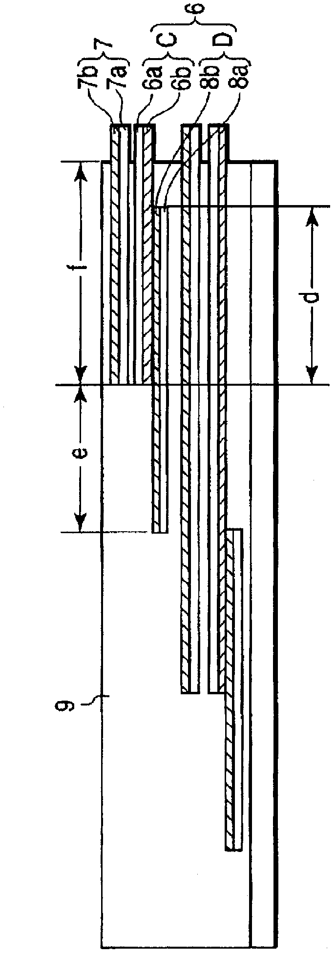
Current terminal structure of superconducting wire material and superconducting cable having this current terminal structure
A technology of superconducting wires and current terminals, which is applied in superconducting devices, superconducting/high-conducting conductors, and the usage of superconducting elements. It can solve problems such as increased connection resistance, large AC loss, and failure to share the same current. Achieve the effect of low connection resistance and less AC loss
- Summary
- Abstract
- Description
- Claims
- Application Information
AI Technical Summary
Problems solved by technology
Method used
Image
Examples
Embodiment 1
[0103] The first superconducting wire rod of the first layer was helically wound on a mold having a diameter of 20 mm formed by kneading wires covered with insulation in multiple layers so that the substrate was on the front side (outer side). In addition, as the first and second superconducting wires, YBCO wires in which a YBCO layer was formed on a substrate made of magnetic Ni5W were used.
[0104] Then, the second superconducting wire rod of the second layer having the same structure as the first superconducting wire rod of the first layer is wound helically so that the surface of the superconducting layer becomes the front side (outer side).
[0105] Afterwards, according to image 3 In the method shown, the ends of the first and second superconducting wires are integrated using a ribbon-shaped solder composed of a connecting wire rod, a mesh tape, and solders 1 to 5 described in Table 1 to obtain figure 1 structure shown. At this time, the type of solder (hereinafter ...
Embodiment 2
[0122] Same as embodiment 1, obtain as figure 1 structure shown. At this time, the relationship between the stripped length (connection length to the soldered and fixed portion) b of the second superconducting wire and the stripped length (connected to the soldered and fixed portion) c of the connecting wire B is changed in various ways. 7 samples were obtained. In addition, one sample was obtained for bc+10 (mm), and b>c+100 (mm). In addition, except for the relationship between b and c at this time, the same conditions as in samples 1-1 to 1-3 of Example 1 were used.
[0123] With regard to these samples, electricity was applied in liquid nitrogen, and the ratios of shunt flow to the first superconducting wire and the second superconducting wire were measured, and the results shown in Table 3 below were obtained.
[0124] table 3
[0125] table 3
[0126] a=50mm
Shunting to the first-layer superconducting wire
Shunting to the second-layer superconduc...
PUM
| Property | Measurement | Unit |
|---|---|---|
| melting point | aaaaa | aaaaa |
Abstract
Description
Claims
Application Information


